

Kyocera Crystal Device Corporation (herein “KCD”*1), a wholly-owned subsidiary of Kyocera Corporation (NYSE:KYO)(TOKYO:6971) specializing in the development and manufacturing of crystal devices, today announced that it has developed the world’s smallest*2 crystal unit for smartphones, wearables, and other electronic devices. The new CX1008 quartz crystal unit measures just 1.0 x 0.8mm yet delivers the same electrical characteristics as Kyocera’s conventional CX1210 model, enabling it to be adopted without circuit board revision. Samples will be available in May 2017 with mass production slated for early 2018.
This Smart News Release features multimedia. View the full release here: http://www.businesswire.com/news/home/20170329005530/en/
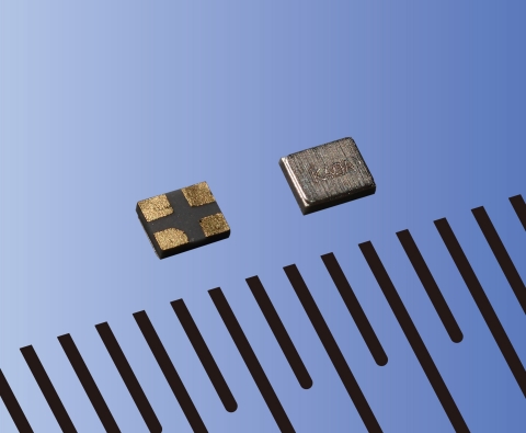
Kyocera Crystal Device's new CX1008 crystal unit (scale: 0.5mm) (Photo: Business Wire)
| Product name | CX1008 | |
| Application | Smartphones, wearable devices | |
| Size | 1.0 X 0.8mm | |
| Height | 0.30mm | |
| Frequency tolerance | ±10ppm | |
| Frequency temperature coefficient | ±10ppm (-30°C to +85°C) | |
CI value (equivalent series | 60Ω MAX (37.4MHz) | |
| Production facility | Shiga Yohkaichi Plant (Japan) | |
Background
Crystal units are used to generate highly stable reference signals in digital circuits, based on the unique material characteristic of quartz to oscillate at a precise frequency when a specific voltage is applied. The trend toward smaller, more functional smartphones and wearable devices requires smaller, better-performing crystal units. Traditionally, however, it was believed that miniaturizing crystal units beyond a certain point would compromise their performance, since electrical characteristics (such as equivalent series resistance) degraded as the device became smaller. However, Kyocera has succeeded in downsizing the crystal unit while maintaining its electrical characteristics — with its current CX1210 (1.2x1.0mm) device, and now, by commercializing the ultra-small CX1008 (1.0x0.8mm) crystal unit. This has been accomplished through crystal element design technology developed exclusively by Kyocera, along with a process that Kyocera developed jointly with Associate Professor Kazuya Yamamura of Osaka University.
Based on this technology, Kyocera will accelerate the development of new low-frequency, high-frequency and high-precision oscillators for such applications as automotive electronics, Advanced Driver Assistance System (ADAS) technologies, IoT devices, wireless network base stations and 5G mobile communications.
Product Features
1.World’s smallest crystal unit with electrical characteristics of the existing CX1210
Downsizing from 1.2x1.0mm to 1.0x0.8mm would ordinarily increase equivalent series resistance (CI value) by approximately 30 percent, requiring circuit board revision. However, by optimizing the design using its own piezoelectric analysis technology, Kyocera has downsized this device to 1.0 x 0.8mm while maintaining the electrical characteristics of the conventional CX1210 crystal unit. This allows the CX1008 to be incorporated into existing circuit designs without revision.
2.Manufacturing Technology
With conventional processes and technologies, a crystal unit exhibits higher levels of variation in key electrical characteristics when produced in smaller dimensions. However, Kyocera has avoided this by applying ultra-high-precision processing (plasma CVM*3 technology) developed with Yamamura. This method, using plasma-generated neutral radicals and a chemical reaction at the surface of an object, enables to control a quartz crystal with highly precise surface conditions and thickness. Further, Kyocera’s proprietary semiconductor processing technology ensures extremely accurate external dimensions, and minimal variation in equivalent series resistance, for optimal performance at reduced size.
*1 KCD will be consolidated into Kyocera Corporation as of April 1,
2017.
*2 Based on research by KCD (as of February 2017)
*3
CVM: Chemical Vaporization Machining
About KYOCERA Crystal Device Corporation
Kyocera Crystal Device Corporation supplies quartz crystal products worldwide, contributing to the development of the ubiquitous networked society. Quartz crystal devices are key components with great influence on the performance of mobile phones, digital cameras and other digital equipment. Kyocera Crystal Device Corporation is one of the world’s leading producers of quartz crystal devices, controlling every aspect of production from growing synthetic quartz crystals to delivering finished products, including quartz crystal units, crystal oscillators, SAW filters and optical devices.
Kyocera Corporation (NYSE:KYO)(TOKYO:6971), the parent and global headquarters of the Kyocera Group, was founded in 1959 as a producer of fine ceramics (also known as “advanced ceramics”). By combining these engineered materials with metals and integrating them with other technologies, Kyocera has become a leading supplier of electronic components, semiconductor packages, mobile phones, printers, copiers, solar power generating systems, cutting tools and industrial ceramics. During the year ended March 31, 2016, the company’s net sales totaled 1.48 trillion yen (approx. USD13.1 billion). Kyocera appears on the “Top 100 Global Innovators” list by Clarivate Analytics and is ranked #531 on Forbes magazine’s 2016 “Global 2000” list of the world’s largest publicly traded companies.
View source version on businesswire.com: http://www.businesswire.com/news/home/20170329005530/en/
Contacts:
KYOCERA Crystal Device Corporation (Japan)
Toru
Fukano, +81-(0)237-43-5747
Corporate Engineering Development
tooru.fukano.xm@kyocera.jp
CONTACT
for media:
KYOCERA Corporation (Japan)
Kenichi Hara,
+81-(0)75-604-3416
Corporate Communications
webmaster.pressgl@kyocera.jp
Fax:
+81-(0)75-604-3516
