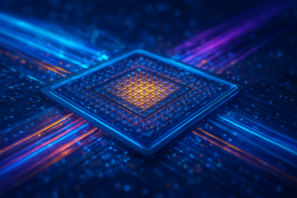
In a move that could fundamentally rewrite the laws of semiconductor physics, Austin-based startup Neurophos has announced a major technological breakthrough with the unveiling of its Tulkas T100 Optical Processing Unit (OPU). By successfully miniaturizing optical modulators to a scale previously thought impossible, Neurophos has created what it calls the "optical transistor"—a device that uses light instead of electricity to perform the massive calculations required for modern artificial intelligence. This development arrives at a critical juncture for the industry as traditional silicon-based chips hit a "thermal wall," struggling to manage the heat and power demands of trillion-parameter AI models.
The announcement coincided with the closing of a $110 million Series A funding round led by Gates Frontier and supported by the venture arm of Microsoft (NASDAQ: MSFT), signaling massive institutional confidence in photonics. Unlike traditional electronic processors that move electrons through copper wires, the Tulkas T100 utilizes silicon photonics and metamaterials to execute matrix-vector multiplications at the speed of light. This shift promises a leap in energy efficiency and compute density that could allow AI data centers to scale far beyond the current limitations of the electrical grid, potentially ending the dominance of pure-electronic architectures.
The Physics of Light: 56 GHz and the 1,000×1,000 Tensor Core
At the heart of the Neurophos breakthrough is a feat of extreme miniaturization. Traditional silicon photonics components, such as Mach-Zehnder Interferometers, are typically bulky—often reaching lengths of 2mm—which has historically prevented them from being packed densely enough to compete with electronic transistors. Neurophos has overcome this by using "meta-atoms" to create metamaterial-based modulators that are 10,000 times smaller than standard photonic elements. This allows the company to tile these optical transistors into a massive 1,000 x 1,000 tensor core on a single die, a significant jump from the 256 x 256 matrices found in the highest-end electronic GPUs.
Because photons do not generate resistive heat in the same way electrons do, the Tulkas T100 can operate at a staggering clock frequency of 56 GHz. This is more than 20 times the boost clock of the most advanced electronic chips currently available. The architecture employs a "compute-in-memory" approach where the weight matrix of an AI model is encoded directly into the metamaterial structure. As light passes through this structure, the mathematical operations are performed nearly instantaneously. This eliminates the "von Neumann bottleneck"—the energy-intensive process of constantly moving data between a processor and external memory—which currently accounts for the majority of power consumption in AI inference.
Initial reactions from the AI research community have been electric. Dr. Aris Silvestris, a senior researcher in photonic computing, noted that "the ability to perform a 1,000-wide matrix multiplication in a single clock cycle at 56 GHz essentially breaks the scaling laws we’ve lived by for forty years." While some experts remain cautious about the challenges of high-precision analog computing, the raw throughput of 470 PetaFLOPS at FP4 precision demonstrated by Neurophos is difficult to ignore. The industry is viewing this not just as an incremental update, but as the first viable "Post-Moore" computing platform.
A New Challenger for the GPU Hegemony
The emergence of the Tulkas T100 represents the first credible threat to the hardware dominance of Nvidia (NASDAQ: NVDA). While Nvidia's recently launched Rubin architecture has pushed the limits of what is possible with electronic CMOS technology, it still relies on scaling through brute-force transistor counts and massive HBM4 memory stacks. Neurophos, by contrast, scales through the physics of light. Internal benchmarks suggest that a single Tulkas OPU can provide 10 times the throughput of an Nvidia Rubin GPU during the "prefill" stage of LLM inference—the most compute-intensive part of processing AI queries—while using a fraction of the power per operation.
For tech giants like Alphabet Inc. (NASDAQ: GOOGL) and Meta Platforms, the strategic advantage of photonics lies in cost-per-flop. As these companies race to deploy autonomous AI agents that require constant, low-latency reasoning, the energy bill for data centers has become a primary bottleneck. By integrating Neurophos OPUs into their infrastructure, hyperscalers could potentially reduce their energy footprint by an order of magnitude. This has spurred a defensive posture from traditional chipmakers; industry analysts suggest that companies like Advanced Micro Devices (NASDAQ: AMD) may soon be forced to accelerate their own internal photonics programs or seek acquisitions in the space to remain competitive.
Crucially, Neurophos has designed its technology to be manufactured using standard CMOS foundry processes. This means they can utilize the existing global supply chain provided by titans like TSMC (NYSE: TSM) and Samsung (KRX: 005930), rather than requiring specialized, exotic fabrication facilities. This "fab-ready" status gives Neurophos a significant time-to-market advantage over other photonic startups that require custom manufacturing. By acting as a high-speed co-processor that can slot into existing data center racks, the Tulkas T100 is positioned not to replace the entire ecosystem overnight, but to capture the most valuable, compute-heavy segments of the AI workload.
Beyond Moore’s Law: Solving the AI Power Crisis
The wider significance of the Neurophos breakthrough cannot be overstated in the context of the global AI landscape. As of early 2026, the primary constraint on AI advancement is no longer just data or algorithmic efficiency, but the availability of electrical power. Data centers are increasingly straining national grids, leading to regulatory scrutiny and environmental concerns. Light-based computing offers a "green" path forward. By achieving 200-300 TOPS/W (Tera-Operations Per Second per Watt), Neurophos is providing an efficiency level that is nearly 20 times higher than the best electronic alternatives.
This development mirrors previous tectonic shifts in computing history, such as the transition from vacuum tubes to the silicon transistor. Just as the transistor allowed for a miniaturization and efficiency leap that vacuum tubes could never match, photonics is poised to do the same for the era of generative AI. However, this transition is not without concerns. Moving from digital electronic signals to optical analog signals introduces new challenges in noise management and error correction. Critics argue that while photonics is superior for raw matrix multiplication, it may still lag behind in the complex branch logic and control flows handled by traditional CPUs and GPUs.
Nevertheless, the environmental impact alone makes the shift toward photonics an inevitability. If the industry can decouple AI performance growth from the linear increase in power consumption, it opens the door for "edge" AI devices—such as highly capable humanoid robots and high-end AR glasses—that can perform trillion-parameter model inference locally without a tether to a power station. The Neurophos milestone is being hailed by many as the "Sputnik moment" for optical computing, proving that light-based logic is no longer a laboratory curiosity but a production-ready reality.
The Road to 2028: Scaling and Software Integration
Looking ahead, the near-term challenge for Neurophos lies in software and system integration. While the hardware specs are dominant, Nvidia’s true "moat" has long been its CUDA software ecosystem. Neurophos is currently working on a compiler stack that allows developers to port PyTorch and JAX models directly to the Tulkas architecture, but the maturity of this software will determine how quickly the industry adopts the new hardware. In the coming 12 to 18 months, expect to see the first large-scale pilot deployments of Neurophos-powered racks in Microsoft Azure and Saudi Aramco (TADAWUL: 2222) data centers.
Long-term, the company aims for full-scale mass production by mid-2028. Experts predict that the next generation of Neurophos chips will move beyond co-processors toward "All-Optical" AI servers, where even the networking and interconnects are handled by integrated photonics. This would eliminate the need for any electronic-to-optical conversion, further slashing latency. The roadmap also includes plans for "heterogeneous" chips that combine a small electronic control core with a massive optical tensor array, providing the best of both worlds.
The primary hurdle remains the packaging of the laser sources. High-performance lasers are sensitive to temperature and aging, and maintaining 56 GHz stability across millions of units will require rigorous engineering. However, if the current trajectory holds, the "Silicon Age" may soon give way to the "Photonics Age." Industry veterans predict that by the end of the decade, the standard metric for AI performance will no longer be transistor count, but "meta-atom density" and "optical bandwidth."
A Pivotal Moment in Computing History
The Neurophos breakthrough marks a definitive end to the era where electronic scaling was the only path to AI progress. By proving that optical transistors can be miniaturized and manufactured at scale, the company has provided a solution to the thermal and energy crises that threatened to stall the AI revolution. The Tulkas T100 OPU is more than just a faster chip; it is a proof-of-concept for an entirely new branch of physics-based computing that leverages the fundamental properties of light to solve the world’s most complex mathematical problems.
As we look toward the remainder of 2026, the key indicators of success will be the results of initial data center benchmarks and the speed of software stack adoption. If Neurophos can deliver on its promise of 100x efficiency gains in real-world environments, the shift toward photonics will accelerate, potentially disrupting the current $100 billion GPU market. This is a moment of profound transformation—a shift from moving particles with mass to moving massless photons, and in doing so, unlocking the next frontier of artificial intelligence.
This content is intended for informational purposes only and represents analysis of current AI developments.
TokenRing AI delivers enterprise-grade solutions for multi-agent AI workflow orchestration, AI-powered development tools, and seamless remote collaboration platforms.
For more information, visit https://www.tokenring.ai/.


