The semiconductor industry is witnessing a profound transformation, driven by an insatiable demand for ever-increasing computational power, particularly from the burgeoning field of artificial intelligence. At the heart of this revolution lies a critical, yet often overlooked, component: the 2D interposer. This advanced packaging technology is rapidly gaining traction, serving as the foundational layer that enables the integration of multiple, diverse chiplets into a single, high-performance package, effectively breaking through the limitations of traditional chip design and paving the way for the next generation of AI accelerators and high-performance computing (HPC) systems.
The acceleration of the 2D interposer market signifies a pivotal shift in how advanced semiconductors are designed and manufactured. By acting as a sophisticated electrical bridge, 2D interposers are dramatically enhancing chip performance, power efficiency, and design flexibility. This technological leap is not merely an incremental improvement but a fundamental enabler for the complex, data-intensive workloads characteristic of modern AI, machine learning, and big data analytics, positioning it as a cornerstone for future technological breakthroughs.
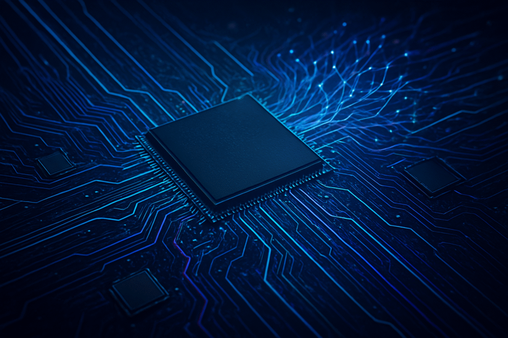
Unpacking the Power: Technical Deep Dive into 2D Interposer Technology
A 2D interposer, particularly in the context of 2.5D packaging, is a flat, typically silicon-based, substrate that serves as an intermediary layer to electrically connect multiple discrete semiconductor dies (often referred to as chiplets) side-by-side within a single integrated package. Unlike traditional 2D packaging, where chips are mounted directly on a package substrate, or true 3D packaging involving vertical stacking of active dies, the 2D interposer facilitates horizontal integration with exceptionally high interconnect density. It acts as a sophisticated wiring board, rerouting connections and spreading them to a much finer pitch than what is achievable on a standard printed circuit board (PCB), thus minimizing signal loss and latency.
The technical prowess of 2D interposers stems from their ability to integrate advanced features such as Through-Silicon Vias (TSVs) and Redistribution Layers (RDLs). TSVs are vertical electrical connections passing completely through a silicon wafer or die, providing a high-bandwidth, low-latency pathway between the interposer and the underlying package substrate. RDLs, on the other hand, are layers of metal traces that redistribute electrical signals across the surface of the interposer, creating the dense network necessary for high-speed communication between adjacent chiplets. This combination allows for heterogeneous integration, where diverse components—such as CPUs, GPUs, high-bandwidth memory (HBM), and specialized AI accelerators—fabricated using different process technologies, can be seamlessly integrated into a single, cohesive system-in-package (SiP).
This approach differs significantly from previous methods. Traditional 2D packaging often relies on longer traces on a PCB, leading to higher latency and lower bandwidth. While 3D stacking offers maximum density, it introduces significant thermal management challenges and manufacturing complexities. 2.5D packaging with 2D interposers strikes a balance, offering near-3D performance benefits with more manageable thermal characteristics and manufacturing yields. Initial reactions from the AI research community and industry experts have been overwhelmingly positive, recognizing 2.5D packaging as a crucial step in scaling AI performance. Companies like TSMC (NYSE: TSM) with its CoWoS (Chip-on-Wafer-on-Substrate) technology have demonstrated how silicon interposers enable unprecedented memory bandwidths, reaching up to 8.6 Tb/s for memory-bound AI workloads, a critical factor for large language models and other complex AI computations.
AI's New Competitive Edge: Impact on Tech Giants and Startups
The rapid acceleration of 2D interposer technology is reshaping the competitive landscape for AI companies, tech giants, and innovative startups alike. Companies that master this advanced packaging solution stand to gain significant strategic advantages. Semiconductor manufacturing behemoths like Taiwan Semiconductor Manufacturing Company (TSMC: TSM), Samsung Electronics (KRX: 005930), and Intel Corporation (NASDAQ: INTC) are at the forefront, heavily investing in their interposer-based packaging technologies. TSMC's CoWoS and InFO (Integrated Fan-Out) platforms, for instance, are critical enablers for high-performance AI chips from NVIDIA Corporation (NASDAQ: NVDA) and Advanced Micro Devices (NASDAQ: AMD), allowing these AI powerhouses to deliver unparalleled processing capabilities for data centers and AI workstations.
For tech giants developing their own custom AI silicon, such as Google (NASDAQ: GOOGL) with its Tensor Processing Units (TPUs) and Amazon (NASDAQ: AMZN) with its Inferentia and Trainium chips, 2D interposers offer a path to optimize performance and power efficiency. By integrating specialized AI accelerators, memory, and I/O dies onto a single interposer, these companies can tailor their hardware precisely to their AI workloads, gaining a competitive edge in cloud AI services. This modular "chiplet" approach facilitated by interposers also allows for faster iteration and customization, reducing the time-to-market for new AI hardware generations.
The disruption to existing products and services is evident in the shift away from monolithic chip designs towards more modular, integrated solutions. Companies that are slow to adopt advanced packaging technologies may find their products lagging in performance and power efficiency. For startups in the AI hardware space, leveraging readily available chiplets and interposer services can lower entry barriers, allowing them to focus on innovative architectural designs rather than the complexities of designing an entire system-on-chip (SoC) from scratch. The market positioning is clear: companies that can efficiently integrate diverse functionalities using 2D interposers will lead the charge in delivering the next generation of AI-powered devices and services.
Broader Implications: A Catalyst for the AI Landscape
The accelerating adoption of 2D interposers fits perfectly within the broader AI landscape, addressing the critical need for specialized, high-performance hardware to fuel the advancements in machine learning and large language models. As AI models grow exponentially in size and complexity, the demand for higher bandwidth, lower latency, and greater computational density becomes paramount. 2D interposers, by enabling 2.5D packaging, are a direct response to these demands, allowing for the integration of vast amounts of HBM alongside powerful compute dies, essential for handling the massive datasets and complex neural network architectures that define modern AI.
This development signifies a crucial step in the "chiplet revolution," a trend where complex chips are disaggregated into smaller, optimized functional blocks (chiplets) that can be mixed and matched on an interposer. This modularity not only drives efficiency but also fosters an ecosystem of specialized IP vendors. The impact on AI is profound: it allows for the creation of highly customized AI accelerators that are optimized for specific tasks, from training massive foundation models to performing efficient inference at the edge. This level of specialization and integration was previously challenging with monolithic designs.
However, potential concerns include the increased manufacturing complexity and cost compared to traditional packaging, though these are being mitigated by technological advancements and economies of scale. Thermal management also remains a significant challenge as power densities on interposers continue to rise, requiring sophisticated cooling solutions. This milestone can be compared to previous breakthroughs like the advent of multi-core processors or the widespread adoption of GPUs for general-purpose computing (GPGPU), both of which dramatically expanded the capabilities of AI. The 2D interposer, by enabling unprecedented levels of integration and bandwidth, is similarly poised to unlock new frontiers in AI research and application.
The Road Ahead: Future Developments and Expert Predictions
Looking ahead, the trajectory of 2D interposer technology is set for continuous innovation and expansion. Near-term developments are expected to focus on further advancements in materials science, exploring alternatives like glass interposers which offer advantages in terms of cost, larger panel sizes, and excellent electrical properties, potentially reaching USD 398.27 million by 2034. Manufacturing processes will also see improvements in yield and cost-efficiency, making 2.5D packaging more accessible for a wider range of applications. The integration of advanced thermal management solutions directly within the interposer substrate will be crucial as power densities continue to climb.
Long-term developments will likely involve tighter integration with 3D stacking techniques, potentially leading to hybrid bonding solutions that combine the benefits of 2.5D and 3D. This could enable even higher levels of integration and shorter interconnects. Experts predict a continued proliferation of the chiplet ecosystem, with industry standards like UCIe (Universal Chiplet Interconnect Express) fostering interoperability and accelerating the development of heterogeneous computing platforms. This modularity will unlock new potential applications, from ultra-compact edge AI devices for autonomous vehicles and IoT to next-generation quantum computing architectures that demand extreme precision and integration.
Challenges that need to be addressed include the standardization of chiplet interfaces, ensuring robust supply chains for diverse chiplet components, and developing sophisticated electronic design automation (EDA) tools capable of handling the complexity of these multi-die systems. Experts predict that by 2030, 2.5D and 3D packaging, heavily reliant on interposers, will become the norm for high-performance AI and HPC chips, with the global 2D silicon interposer market projected to reach US$2.16 billion. This evolution will further blur the lines between traditional chip design and system-level integration, pushing the boundaries of what's possible in artificial intelligence.
Wrapping Up: A New Era of AI Hardware
The acceleration of the 2D interposer market marks a significant inflection point in the evolution of AI hardware. The key takeaway is clear: interposers are no longer just a niche packaging solution but a fundamental enabler for high-performance, power-efficient, and highly integrated AI systems. They are the unsung heroes facilitating the chiplet revolution and the continued scaling of AI capabilities, providing the necessary bandwidth and low latency for the increasingly complex models that define modern artificial intelligence.
This development's significance in AI history is profound, representing a shift from solely focusing on transistor density (Moore's Law) to emphasizing advanced packaging and heterogeneous integration as critical drivers of performance. It underscores the fact that innovation in AI is not just about algorithms and software but equally about the underlying hardware infrastructure. The move towards 2.5D packaging with 2D interposers is a testament to the industry's ingenuity in overcoming physical limitations to meet the insatiable demands of AI.
In the coming weeks and months, watch for further announcements from major semiconductor manufacturers and AI companies regarding new products leveraging advanced packaging. Keep an eye on the development of new interposer materials, the expansion of the chiplet ecosystem, and the increasing adoption of these technologies in specialized AI accelerators. The humble 2D interposer is quietly, yet powerfully, laying the groundwork for the next generation of AI breakthroughs, shaping a future where intelligence is not just artificial, but also incredibly efficient and integrated.
This content is intended for informational purposes only and represents analysis of current AI developments.
TokenRing AI delivers enterprise-grade solutions for multi-agent AI workflow orchestration, AI-powered development tools, and seamless remote collaboration platforms.
For more information, visit https://www.tokenring.ai/.