In a landmark series of developments culminating in late 2025, researchers have successfully engineered artificial semiconductor honeycomb lattices (ASHLs) with fully tunable energy band structures, marking a pivotal shift in the race for fault-tolerant quantum computing. By manipulating the geometry and composition of these "designer materials" at the atomic scale, scientists have moved beyond merely mimicking natural substances like graphene, instead creating entirely new electronic landscapes—including rare "quartic" energy dispersions—that do not exist in nature.
The immediate significance of this breakthrough cannot be overstated. For decades, the primary hurdle in quantum computing has been "noise"—the environmental interference that causes qubits to lose their quantum state. By engineering these artificial lattices to host topological states, researchers have effectively created "quantum armor," allowing information to be stored in the very shape of the electron's path rather than just its spin or charge. This development bridges the gap between theoretical condensed matter physics and the multi-billion-dollar semiconductor manufacturing industry, signaling the end of the experimental era and the beginning of the "semiconductor-native" quantum age.
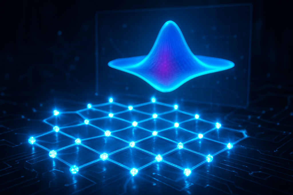
Engineering the "Mexican Hat": The Technical Leap
The technical core of this advancement lies in the transition from planar to "staggered" honeycomb lattices. Researchers from the Izmir Institute of Technology and Bilkent University recently demonstrated that by introducing a vertical, out-of-plane displacement between the sublattices of a semiconductor heterostructure, they could amplify second-nearest-neighbor coupling. This geometric "staggering" allows for the creation of quartic energy bands—specifically a "Mexican-hat-shaped" (MHS) dispersion—where the density of electronic states becomes exceptionally high at specific energy levels known as van Hove singularities.
Unlike traditional semiconductors where electrons behave like standard particles, or graphene where they mimic massless light (Dirac fermions), electrons in these quartic lattices exhibit a flat-bottomed energy profile. This allows for unprecedented control over electron-electron interactions, enabling the study of strongly correlated phases and exotic magnetism. Concurrently, a team at New York University (NYU) and the University of Queensland achieved a parallel breakthrough by creating a superconducting version of germanium. Using Molecular Beam Epitaxy (MBE) to "hyperdope" germanium with gallium atoms, they integrated 25 million Josephson junctions onto a single 2-inch wafer. This allows for the monolithic integration of classical logic and quantum qubits on the same chip, a feat previously thought to be decades away.
These advancements differ from previous approaches by moving away from "noisy" intermediate-scale quantum (NISQ) devices. Earlier attempts relied on natural materials with fixed properties; the 2025 breakthrough allows engineers to "dial in" the desired bandgap and topological properties during the fabrication process. The research community has reacted with overwhelming optimism, with experts noting that the ability to tune these bands via mechanical strain and electrical gating provides the "missing knobs" required for scalable quantum hardware.
The Industrial Realignment: Microsoft, Intel, and the $5 Billion Pivot
The ripple effects of these breakthroughs have fundamentally altered the strategic positioning of major tech giants. Microsoft (NASDAQ: MSFT) has emerged as an early leader in the "topological" space, announcing its Majorana 1 quantum chip in February 2025. Developed at the Microsoft Quantum Lab in partnership with Purdue University, the chip utilizes artificial semiconductor-superconductor hybrid lattices to stabilize Majorana zero modes. Microsoft is positioning this as the "transistor of the quantum age," claiming it will enable a one-million-qubit Quantum Processing Unit (QPU) that can be seamlessly integrated into its existing Azure cloud infrastructure.
Intel (NASDAQ: INTC), meanwhile, has leveraged its decades of expertise in silicon and germanium to pivot toward spin-based quantum dots. The recent NYU breakthrough in superconducting germanium has validated Intel’s long-term bet on Group IV elements. In a stunning market move in September 2025, NVIDIA (NASDAQ: NVDA) announced a $5 billion investment in Intel to co-design hybrid AI-quantum chips. NVIDIA’s goal is to integrate its NVQLink interconnect technology with Intel’s germanium-based qubits, creating a unified architecture where Blackwell GPUs handle real-time quantum error correction.
This development poses a significant challenge to companies focusing on traditional superconducting loops, such as IBM (NYSE: IBM). While IBM has successfully transitioned to 300mm wafer technology for its "Nighthawk" processors, the "topological protection" offered by artificial lattices could potentially render non-topological architectures obsolete due to their higher error-correction overhead. The market is now witnessing a fierce competition for "foundry-ready" quantum designs, with the US government taking a 10% stake in Intel earlier this year to ensure domestic control over these critical semiconductor-quantum hybrid technologies.
Beyond the Transistor: A New Paradigm for Material Science
The wider significance of artificial honeycomb lattices extends far beyond faster computers; it represents a new paradigm for material science. In the broader AI landscape, the bottleneck is no longer just processing power, but the energy efficiency of the hardware. The correlated topological insulators enabled by these lattices allow for "dissipationless" edge transport—meaning electrons can move without generating heat. This could lead to a new generation of "Green AI" hardware that consumes a fraction of the power required by current H100 or B200 clusters.
Historically, this milestone is being compared to the 1947 invention of the point-contact transistor. Just as that discovery moved electronics from fragile vacuum tubes to solid-state reliability, artificial lattices are moving quantum bits from fragile, laboratory-bound states to robust, chip-integrated components. However, concerns remain regarding the "quantum divide." The extreme precision required for Molecular Beam Epitaxy and 50nm-scale lithography means that only a handful of foundries globally—primarily Taiwan Semiconductor Manufacturing Company (NYSE: TSM) and Intel—possess the capability to manufacture these chips, potentially centralizing quantum power in a few geographic hubs.
Furthermore, the ability to simulate complex molecular interactions using these "designer lattices" is expected to accelerate drug discovery and carbon capture research. By mapping the energy bands of a theoretical catalyst onto an artificial lattice, researchers can "test" the material's properties in a simulated quantum environment before ever synthesizing it in a chemistry lab.
The Road to 2030: Room Temperature and Wafer-Scale Scaling
Looking ahead, the next frontier is the elimination of the "dilution refrigerator." Currently, most quantum systems must be cooled to near absolute zero. However, researchers at Purdue University have already demonstrated room-temperature spin qubits in germanium disulfide lattices. The near-term goal for 2026-2027 is to integrate these room-temperature components into the staggered honeycomb architectures perfected this year.
The industry also faces the challenge of "interconnect density." While the NYU team proved that 25 million junctions can fit on a wafer, the wiring required to control those junctions remains a massive engineering hurdle. Experts predict that the next three years will see a surge in "cryo-CMOS" development—classical control electronics that can operate at the same temperatures as the quantum chip, effectively merging the two worlds into a single, cohesive package. If successful, we could see the first commercially viable, fault-tolerant quantum computers by 2028, two years ahead of previous industry roadmaps.
Conclusion: The Year Quantum Became "Real"
The breakthroughs in artificial semiconductor honeycomb lattices and tunable energy bands mark 2025 as the year quantum computing finally found its "native" substrate. By moving beyond the limitations of natural materials and engineering the very laws of electronic dispersion, researchers have provided the industry with a scalable, foundries-compatible path to the quantum future.
The key takeaways are clear: the convergence of semiconductor manufacturing and quantum physics is complete. The strategic alliance between NVIDIA and Intel, the emergence of Microsoft’s topological "topoconductor," and the engineering of "Mexican-hat" energy bands all point to a singular conclusion: the quantum age will be built on the back of the semiconductor industry. In the coming months, watch for the first "hybrid" cloud instances on Azure and AWS that utilize these artificial lattice chips for specialized optimization tasks, marking the first true commercial applications of this groundbreaking technology.
This content is intended for informational purposes only and represents analysis of current AI and semiconductor developments as of December 22, 2025.
TokenRing AI delivers enterprise-grade solutions for multi-agent AI workflow orchestration, AI-powered development tools, and seamless remote collaboration platforms.
For more information, visit https://www.tokenring.ai/.