Aeluma and Thorlabs Unveil Breakthrough with Large-Diameter Wafer Manufacturing Platform for Quantum Computing and Communication
Successful Demonstration Shows Promise for High-Performance and Mass-Manufacturable Quantum Photonic Circuits on Silicon
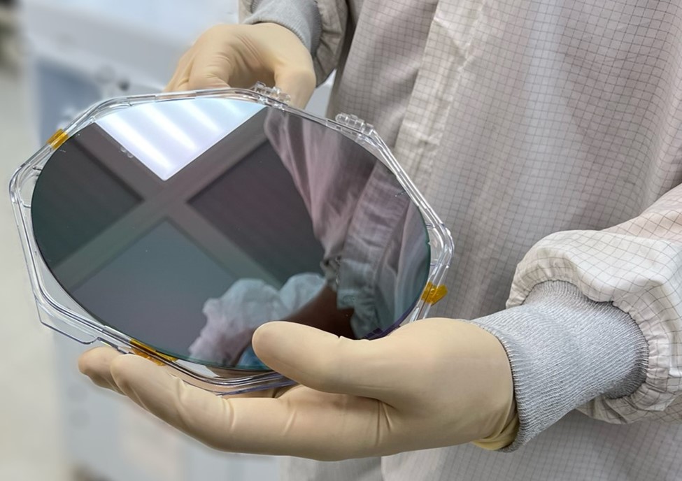
GOLETA, CA / ACCESS Newswire / May 29, 2025 / Aeluma, Inc. (NASDAQ: ALMU), a semiconductor company specializing in high-performance, scalable technologies, together with Thorlabs, a vertically integrated photonics products manufacturer, today announced a major advancement in silicon photonics that could accelerate adoption of quantum computing and communication at commercial scale.
Aeluma's large-diameter wafer platform combines the performance of compound semiconductors with the scale of mainstream silicon manufacturing, enabling cost-effective solutions across high-growth markets including mobile, AI, defense and aerospace, automotive, and quantum computing.
Silicon photonics is a promising technology for quantum computing and communication. Aeluma's ability to incorporate quantum dot sources and highly nonlinear electro-optic materials unlocks new high-performance functionality for this platform.
Collaborating with Thorlabs, and with support from the Office of Secretary of Defense, Aeluma successfully demonstrated wafer-scale integration of aluminum gallium arsenide, a nonlinear optical material, onto CMOS silicon photonics standard 200mm diameter wafers, providing a path for scaling complex quantum photonic circuits.
The nonlinear optical material enables entangled photon pair generation and modulation, key building blocks for quantum photonic systems. Compared with other materials like silicon nitride or lithium niobate, aluminum gallium arsenide offers significantly improved efficiency for next-generation quantum photonic circuits.
"Scalable photonic integration is essential to move quantum technologies out of the lab and into real-world systems," said Matthew Dummer, Ph.D., Director of Technology at Aeluma. "By merging the performance of compound semiconductors with the scalability of silicon photonics, we are pushing the boundaries of what's possible in quantum and AI."
This combination of advanced materials and CMOS silicon substrates, using manufacturing methods compatible with mainstream fabs, marks a step toward volume production, which could move quantum technologies out of research labs and into mass-market products.
"This successful collaboration was enabled by the large-area epitaxial growth capabilities of Aeluma and the direct wafer bonding expertise at Thorlabs," added Garrett Cole, Ph.D., Manager of Thorlabs Crystalline Solutions. "The heterogeneous integration of compound semiconductor materials on silicon is broadly applicable and now shows significant promise for quantum photonics."
The breakthrough demonstration complements Aeluma's work with quantum dot materials in 300mm silicon photonics, aimed at optical interconnects for AI infrastructure and advanced sensing. It directly addresses a longstanding challenge in scaling quantum photonic systems and could provide a meaningful step forward for quantum system integrators pursuing scalable, production-ready solutions.
About Aeluma
Aeluma (www.aeluma.com) develops photonics and optoelectronics for sensing, computing, and communication applications. Aeluma has pioneered a technique to manufacture semiconductor chips using high-performance compound semiconductor materials on large-diameter substrates that are commonly used for mass-market microelectronics. The technology has the potential to enhance performance and scale manufacturing, both of which are critical for emerging applications. Aeluma is developing a streamlined business model from its headquarters in Santa Barbara, California that has a state-of-the-art manufacturing cleanroom. Its transformative semiconductor chip technology may impact a variety of markets including mobile, defense and aerospace, AI, automotive, AR/VR, quantum, and communication. Aeluma differentiates itself with unique semiconductor manufacturing capability, proprietary technology, the ability to perform rapid prototyping, and a broad set of product offerings.
About Thorlabs
Thorlabs, a vertically integrated photonics products manufacturer, was founded in 1989 to serve the laser and electro-optics research market. As that market has spawned a multitude of technical innovations, Thorlabs has extended its core competencies in an effort to play an ever-increasing role to serve the Photonics Industry at the research end, as well as the industrial, life science, medical, and defense segments. The organization's highly integrated and diverse manufacturing assets include semiconductor fabrication of Fabry-Perot, DFB, and VCSEL lasers; fiber towers for drawing both silica and fluoride glass optical fibers; MBE/MOCVD epitaxial wafer growth reactors; extensive glass and metal fabrication facilities; advanced thin film deposition capabilities; and optomechanical and optoelectronic shops. Thorlabs is headquartered in Newton, New Jersey, and Thorlabs Crystalline Solutions is based in Santa Barbara, California.
Aeluma Forward-Looking Statements
All statements in this press release that are not historical are forward-looking statements, including, among other things, statements relating to the Company's expectations regarding its market position and market opportunity, expectations and plans as to its product development, manufacturing and sales, and relations with its partners and investors. These statements are not historical facts but rather are based on the Company's current expectations, estimates, and projections regarding its business, operations and other similar or related factors. Words such as "may," "will," "could," "would," "should," "anticipate," "predict," "potential," "continue," "expect," "intend," "plan," "project," "believe," "estimate," and other similar or related expressions are used to identify these forward-looking statements, although not all forward-looking statements contain these words. You should not place undue reliance on forward-looking statements because they involve known and unknown risks, uncertainties, and assumptions that are difficult or impossible to predict and, in some cases, beyond the Company's control. Actual results may differ materially from those in the forward-looking statements as a result of a number of factors, including those described in the Company's filings with the Securities and Exchange Commission. The Company undertakes no obligation to revise or update information in this release to reflect events or circumstances in the future, even if new information becomes available.
Aeluma Contact:
Aeluma, Inc.
(805) 351-2707
info@aeluma.com
Aeluma Investor Contact:
Bishop IR
Mike Bishop
(415) 894-9633
ir@aeluma.com
SOURCE: Aeluma, Inc.
View the original press release on ACCESS Newswire
If you believe this article contains misleading, harmful, or spam content, please let us know.
Report this articleMore News
View More


Recent Quotes
View MoreQuotes delayed at least 20 minutes.
By accessing this page, you agree to the Privacy Policy and Terms Of Service.