Keysight Accelerates Silicon Photonics Wafer Production with Fully Automated One-stop Test Solution
Delivers quick volume production launch with stability and repeatability
Keysight Technologies, Inc. (NYSE: KEYS), a leading technology company that delivers advanced design and validation solutions to help accelerate innovation to connect and secure the world, announced the new NX5402A Silicon Photonics Test System integrated with Keysight PathWave Semiconductor Test software technology (part of Keysight PathWave Test software), which enables semiconductor manufacturers to speed delivery of silicon photonics wafer production with stable and repeatable test capabilities.
This press release features multimedia. View the full release here: https://www.businesswire.com/news/home/20210907005598/en/
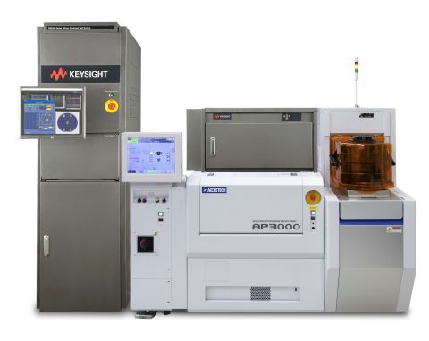
Keysight's NX5402A Silicon Photonics Test System with Accretech’s AP3000 Wafer Prober. (Photo: Business Wire)
Silicon photonics is one of the key emerging technologies addressing growing internet traffic and demand for higher data rate. Silicon photonics’ primary applications are in the data center market, driven by big data and cloud applications, but it is expected to be used in other areas, including healthcare, automotive Light Detection and Ranging (LiDAR), optical computing and quantum computing.
According to a recent market research report by Yole Développement, the overall silicon photonics market will reach US$3.9 billion in 2025. As a result, many manufacturers are considering silicon photonics fabrication. However, there has not been any commercially available silicon photonics testing equipment for mass production using fully automated wafer probers. In addition, silicon photonics testing requires a variety of sensitive and accurate measurements. Companies and system integrators are pursuing system optimization and maintenance due to complex and inefficient communications with multiple vendors.
"Ahead of the growing market demand for silicon photonics, Keysight is excited to announce the first test solution for silicon photonics volume production market,” said Shinji Terasawa, vice president and general manager of Keysight’s Wafer Test Solutions group. “Our NX5402A test system is the first solution that combines Keysight’s expertise in electrical and optical measurement with Keysight’s fiber alignment and positioning system integrated by PathWave Semiconductor Test software."
Keysight's new NX5402A Silicon Photonics test system delivers the following key customer benefits:
- One-stop: Provides proven measurement technologies and direct support capabilities including integrated optical and electrical test capabilities and Keysight-developed fiber alignment and positioning system based on Keysight’s measurement science.
- Fully automated: Eliminates manual operations with PathWave Semiconductor Test software which is compatible with Keysight’s SPECS software, enabling one-pass silicon photonics testing.
- Volume production ready: Factory automation software, safety interlock and clean room ready features support manufacturing use, providing high throughput testing based on multi-channel optical and electrical test architecture, as well as optimized fiber alignment.
- Demonstrated system performance: Maintains high accuracy, repeatability and reproducibility from laboratory to fabrication, delivering advanced wafer-level photonic calibration, as well as reliable performance monitoring with built-in automatic system diagnostics.
About Keysight Technologies
Keysight delivers advanced design and validation solutions that help accelerate innovation to connect and secure the world. Keysight’s dedication to speed and precision extends to software-driven insights and analytics that bring tomorrow’s technology products to market faster across the development lifecycle, in design simulation, prototype validation, automated software testing, manufacturing analysis, and network performance optimization and visibility in enterprise, service provider and cloud environments. Our customers span the worldwide communications and industrial ecosystems, aerospace and defense, automotive, energy, semiconductor and general electronics markets. Keysight generated revenues of $4.2B in fiscal year 2020. For more information about Keysight Technologies (NYSE: KEYS), visit us at www.keysight.com.
Additional information about Keysight Technologies is available in the newsroom at https://www.keysight.com/go/news and on Facebook, LinkedIn, Twitter and YouTube.
View source version on businesswire.com: https://www.businesswire.com/news/home/20210907005598/en/
Contacts
Geri Lynne LaCombe, Americas/Europe
+1 303 662 4748
geri_lacombe@keysight.com
Fusako Dohi, Asia
+81 42 660-2162
fusako_dohi@keysight.com
If you believe this article contains misleading, harmful, or spam content, please let us know.
Report this articleMore News
View More


Recent Quotes
View MoreQuotes delayed at least 20 minutes.
By accessing this page, you agree to the Privacy Policy and Terms Of Service.