Samsung Electronics and NAVER Team Up to Develop Semiconductor Solutions Optimized for Hyperscale AI
The two companies intend to combine semiconductor design and manufacturing prowess with proven AI capabilities to maximize the speed and power efficiency of large-scale AI models
Samsung Electronics Co., Ltd., the world leader in advanced memory technology, and NAVER Corporation, a global internet company with top-notch AI technology, today announced a wide-reaching collaboration to develop semiconductor solutions tailored for hyperscale artificial intelligence (AI) models. Leveraging Samsung’s next-generation memory technologies like computational storage, processing-in-memory (PIM) and processing-near-memory (PNM), as well as Compute Express Link (CXL), the companies intend to pool their hardware and software resources to dramatically accelerate the handling of massive AI workloads.
This press release features multimedia. View the full release here: https://www.businesswire.com/news/home/20221205005465/en/
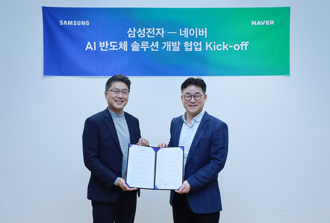
Jinman Han, Executive Vice President of Memory Global Sales & Marketing at Samsung Electronics (left), and Suk Geun Chung, Head of NAVER CLOVA CIC (right), at ceremony for signing of Memorandum of Understanding. (Photo: Business Wire)
Recent advances in hyperscale AI have led to an exponential growth in data volumes that need to be processed. However, the performance and efficiency limitations of current computing systems pose significant challenges in meeting these heavy computational requirements, fueling the need for new AI-optimized semiconductor solutions.
Developing such solutions requires an extensive convergence of semiconductor and AI disciplines. Samsung is combining its semiconductor design and manufacturing expertise with NAVER’s experience in the development and verification of AI algorithms and AI-driven services, to create solutions that take the performance and power efficiency of large-scale AI to a new level.
For years, Samsung has been introducing memory and storage that support high-speed data processing in AI applications, from computational storage (SmartSSD) and PIM-enabled high bandwidth memory (HBM-PIM) to next-generation memory supporting the Compute Express Link (CXL) interface. Samsung will now join with NAVER to optimize these memory technologies in advancing large-scale AI systems.
NAVER will continue to refine HyperCLOVA, a hyperscale language model with over 200 billion parameters, while improving its compression algorithms to create a more simplified model that significantly increases computation efficiency.
“Through our collaboration with NAVER, we will develop cutting-edge semiconductor solutions to solve the memory bottleneck in large-scale AI systems,” said Jinman Han, Executive Vice President of Memory Global Sales & Marketing at Samsung Electronics. “With tailored solutions that reflect the most pressing needs of AI service providers and users, we are committed to broadening our market-leading memory lineup including computational storage, PIM and more, to fully accommodate the ever-increasing scale of data.”
“Combining our acquired knowledge and know-how from HyperCLOVA with Samsung’s semiconductor manufacturing prowess, we believe we can create an entirely new class of solutions that can better tackle the challenges of today’s AI technologies,” said Suk Geun Chung, Head of NAVER CLOVA CIC. “We look forward to broadening our AI capabilities and bolstering our edge in AI competitiveness through this strategic partnership.”
About Samsung Electronics Co., Ltd.
Samsung inspires the world and shapes the future with transformative ideas and technologies. The company is redefining the worlds of TVs, smartphones, wearable devices, tablets, digital appliances, network systems, and memory, system LSI, foundry and LED solutions. For the latest news, please visit the Samsung Newsroom at news.samsung.com.
View source version on businesswire.com: https://www.businesswire.com/news/home/20221205005465/en/
Contacts
John Lucas
for Samsung Semiconductor, Inc.
j.lucas@partner.samsung.com
If you believe this article contains misleading, harmful, or spam content, please let us know.
Report this articleMore News
View More

Recent Quotes
View MoreQuotes delayed at least 20 minutes.
By accessing this page, you agree to the Privacy Policy and Terms Of Service.