Renesas Develops Circuit Technologies for 22-nm Embedded STT-MRAM with Faster Read and Write Performance for MCUs in IoT Applications
Announced at 2022 Symposium on VLSI: Achieving 5.9 ns Random Read Access and 5.8 MB/s Write Throughput on Test Chip
Renesas Electronics Corporation (TSE:6723), a premier supplier of advanced semiconductor solutions, today announced that it has developed circuit technologies for an embedded spin-transfer torque magnetoresistive random-access memory (STT-MRAM, hereinafter MRAM) test chip with fast read and write operations fabricated using a 22-nm process. The test chip includes a 32-megabit (Mbit) embedded MRAM memory cell array and achieves 5.9-nanosecond (ns) random read access at a maximum junction temperature of 150°C, and a write throughput of 5.8-megabyte-per-second (MB/s).
This press release features multimedia. View the full release here: https://www.businesswire.com/news/home/20220616005322/en/
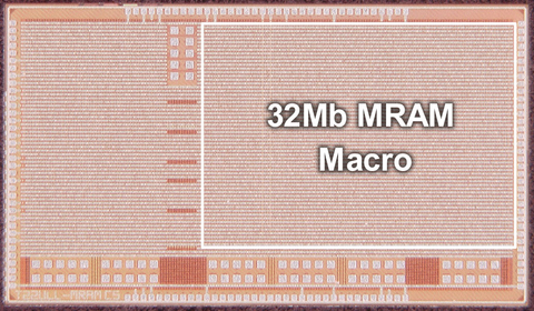
Renesas STT-MRAM test chip with fast read and write operations (Graphic: Business Wire)
Renesas presented these achievements on June 16 at the 2022 IEEE Symposium on VLSI Technology and Circuits, held between June 12 and 17 in Hawaii.
As the advances of IoT and AI technologies continue, microcontroller units (MCUs) used in endpoint devices are expected to deliver higher performance than ever, and therefore need to be fabricated with finer process nodes. MRAM fabricated in BEOL (Note 1) is advantageous compared to flash memory fabricated in FEOL (Note 2) for sub-22 nm processes because it is compatible with existing CMOS logic process technology and requires fewer additional mask layers. However, MRAM has a smaller read margin than flash memory, which degrades read speed. A large gap between the CPU operating frequency and the read frequency of the non-volatile memory is also a challenge since it can degrade MCU performance.
MRAM can also achieve shorter write time than flash memory because it requires no erase operation before write operation. However, further speed improvements are needed to shorten system downtime for over-the-air (OTA) updates required for endpoint devices and reduce costs for end product manufacturers in writing control codes for MCUs.
To address these challenges and respond to market demand for higher MCU performance, Renesas has developed the following new circuit technologies to achieve faster read and write operation in MRAM.
1. Fast Read Technology Employing High-Precision Sense Amplifier Circuit
MRAM uses memory cells including magnetic tunnel junction (MTJ) devices in which high and low-resistance states correspond to data values of 1 and 0 respectively to store information. A differential sense amplifier distinguishes between the two states by reading the voltage difference in discharge speed between the memory cell current and reference current. However, since the memory cell current difference between the 1 and 0 states is smaller for MRAM than for flash memory, the voltage difference read by the sense amplifier is smaller. Even if the discharge time is extended to wider voltage differences between the differential input nodes of the sense amplifier, both of the input nodes are susceptible to being completely discharged before securing a necessary voltage difference. This problem is particularly acute at high temperatures.
To resolve this issue, Renesas introduced a new technology utilizing capacitive coupling to boost the voltage level of the differential input nodes, allowing the differential amplifier to sense a voltage difference even when the memory cell current difference is small, achieving high-precision and fast read operation.
2. Fast Write Technology with Simultaneous Write Bit Number Optimization and Shortened Mode Transition Time
Following the high-speed write technologies for embedded STT-MRAM announced in December 2021, the new technology achieves even higher speed by shortening the mode transition time during write operation.
This technology divides up the areas to which write voltage is applied and, by inputting the write address before the write voltage setup, it selectively applies voltage only to the necessary area. This method reduces the parasitic capacitive load on the area where the voltage is applied during the write operation, reducing the voltage setup time. As a result, the mode transition time to write operation is reduced by approximately 30%, speeding up write operation.
Renesas continues to develop technologies aimed at the application of embedded MRAM technology in MCU products. These new technologies have the potential to dramatically boost memory access speed, which is currently a challenge with MRAM, to exceed 100 MHz, enabling higher-performance MCUs with embedded MRAM. Faster write speed will contribute to more efficient code writing to endpoint devices. Renesas is committed to further increasing capacity, speed, and power efficiency for MCUs to accommodate a range of new applications.
Notes
1. BEOL stands for “back end of line” and designates the latter portion of semiconductor fabrication from deposition of metal interconnect layers to completion.
2. FEOL stands for “front end of line” and designates the first portion of semiconductor fabrication where devices are patterned in the substrate and before the deposition of metal interconnect layers.
About Renesas Electronics Corporation
Renesas Electronics Corporation (TSE: 6723) empowers a safer, smarter and more sustainable future where technology helps make our lives easier. A leading global provider of microcontrollers, Renesas combines our expertise in embedded processing, analog, power and connectivity to deliver complete semiconductor solutions. These Winning Combinations accelerate time to market for automotive, industrial, infrastructure and IoT applications, enabling billions of connected, intelligent devices that enhance the way people work and live. Learn more at renesas.com. Follow us on LinkedIn, Facebook, Twitter, YouTube and Instagram
(Remarks). All names of products or services mentioned in this press release are trademarks or registered trademarks of their respective owners.
View source version on businesswire.com: https://www.businesswire.com/news/home/20220616005322/en/
Contacts
Americas
Don Parkman
Renesas Electronics Corporation
+ 1-408-887-4308
don.parkman.xh@renesas.com
More News
View More


Recent Quotes
View More
Quotes delayed at least 20 minutes.
By accessing this page, you agree to the Privacy Policy and Terms Of Service.