Keysight Introduces PCIe Designer and Chiplet PHY Designer for Digital Standards-Driven Simulation Workflows
- Improves PCIe design productivity using a smarter and streamlined workflow with simulation-driven virtual compliance test solutions
- Supports design exploration and report generation that speeds chiplet signal integrity analysis and UCIe compliance verification to increase designer productivity and time-to-market
Keysight Technologies, Inc. (NYSE: KEYS) introduces PCIe Designer, a new product in the Advanced Design System (ADS) product suite that supports simulation workflows based on industry standards for high-speed, high-frequency digital designs. PCIe Designer is an intelligent design environment for modeling and simulating the latest Peripheral Component Interconnect Express (PCIe) Gen5 and Gen6 systems. Keysight is also improving its electronic design automation (EDA) platform by adding new features to the existing Chiplet PHY Designer tool to estimate chiplet die-to-die link margin performance and Voltage Transfer Function (VTF) compliance measurement.
This press release features multimedia. View the full release here: https://www.businesswire.com/news/home/20240718842236/en/
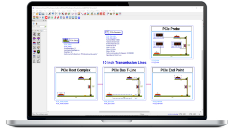
PCIe Designer is an intelligent design environment for modeling and simulating the latest PCIe Gen5 and Gen6 systems. (Graphic: Business Wire)
PCIe is a versatile and essential interface standard across a wide range of electronics industry segments due to its high-speed data transfer capabilities, scalability, and adaptability. Adoption spans from everyday consumer electronics to specialized applications in high-performance computing and critical infrastructure systems.
Complex PCIe designs support multi-link and multi-lane systems that involve a complex analysis setup between RootComplex and End-Point, sometimes incorporating mid-channel repeaters. Designers spend an inordinate amount of time preparing simulations that are prone to mistakes. Simulations often lack vendor-specific algorithmic modeling interface (AMI) simulation models, which are required early in the design cycle for design space exploration. Designers also need assurance that their prototype design will pass compliance testing before hardware fabrication.
Productivity, Workflow, and Compliance Improvement Features
- The PCIe Designer automates the setup for multi-link, multi-lane, and multi-level (PAM4) PCIe systems using a smart design environment. It simplifies simulation setup and reduces time-to-first-insight.
- The PCIe AMI modeler, which supports NRZ and PAM4 modulations, facilitates quick AMI model generation needed for PCIe system analysis. The AMI Model Builder gives designers a wizard-driven AMI model generation workflow to rapidly create models for both transmitters (Tx) and receivers (Rx).
- Streamlined, simulation-driven virtual compliance testing enables designers to ensure design quality. The integrated, simulation-driven PCIe compliance test workflow reduces design costs by minimizing design iterations and shortening time-to-market.
Chiplet PHY Designer Enhancements
- Chiplet PHY Designer is the EDA industry’s first simulation solution for Universal Chiplet Interconnect Express (UCIe) standards, enabling predictions of die-to-die link margin, VTF for channel compliance analysis, and forwarded clock capability. Chiplet PHY Designer includes new design exploration and report generation features that accelerate signal integrity analysis and compliance verification to improve designer productivity and time-to-market.
Hee-Soo Lee, Director of High-Speed Digital segment, Keysight EDA, said, “We continue to expand our standards-driven workflow approach to support our customers. Our high-speed digital product portfolio is leading the EDA industry with the most accurate and advanced simulation software for signal integrity analysis and compliance test validation. Digital standards such as PCIe and UCIe are critical to the performance of electronic systems. Designers using our PCIe and UCIe simulation solutions in their workflows can shift left their development cycle to save significant time and cost.”
More Information: July 24th Webinar
To learn more about the newest 2024 additions to Keysight’s Chiplet PHY Designer and PCIe Designer please join the Keysight EDA webinar on July 24th. For more information and to register for the event, visit Standards Driven EDA Workflows webinar page.
Resources
- W3651B PCIe Designer
- W3650B Chiplet PHY Designer
- PCIe and Chiplet PHY Designer Solutions
- Webinar: Simplify Design Verification and Compliance with Standards-Driven EDA Workflows
About Keysight Technologies
At Keysight (NYSE: KEYS), we inspire and empower innovators to bring world-changing technologies to life. As an S&P 500 company, we’re delivering market-leading design, emulation, and test solutions to help engineers develop and deploy faster, with less risk, throughout the entire product life cycle. We’re a global innovation partner enabling customers in communications, industrial automation, aerospace and defense, automotive, semiconductor, and general electronics markets to accelerate innovation to connect and secure the world. Learn more at Keysight Newsroom and www.keysight.com.
View source version on businesswire.com: https://www.businesswire.com/news/home/20240718842236/en/
Contacts
Paul Erwin
Americas
+1 248 430–9075
paul.erwin@keysight.com
Fusako Dohi
Asia
+81 42 660-2162
fusako_dohi@keysight.com
Jenny Gallacher
Europe
+44 (0) 7800 737 982
jenny.gallacher@keysight.com
If you believe this article contains misleading, harmful, or spam content, please let us know.
Report this articleMore News
View More


Recent Quotes
View MoreQuotes delayed at least 20 minutes.
By accessing this page, you agree to the Privacy Policy and Terms Of Service.