TSMC and Cadence Collaborate to Deliver AI-Driven Advanced-Node Design Flows, Silicon-Proven IP and 3D-IC Solutions
Highlights:
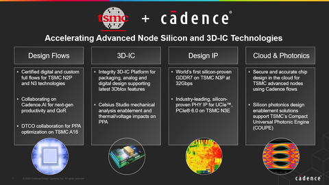
- AI-driven digital and custom design flows available for the latest TSMC N2P and N3 technologies
- Cadence is collaborating with TSMC on A16 design solutions to optimize PPA
- Cadence Integrity 3D-IC Platform unifying packaging, analog and digital design supports latest 3Dblox features
- Collaboration includes Celsius Studio mechanical analysis enablement and thermal/voltage impacts on power/IR/STA and what-if in-design analysis
- Design IP powers the AI factory, including the industry’s first silicon-proven GDDR7 IP running at 32Gbps on the TSMC N3 technology
- Cadence solutions support secure chip design in the cloud, with design solutions to support TSMC silicon photonics technologies
Cadence Design Systems, Inc. (Nasdaq: CDNS) today announced that it is collaborating with TSMC to enhance productivity and optimize product performance for AI-driven advanced-node designs and 3D-ICs. The rapid adoption of AI applications has created unprecedented demand for advanced silicon solutions capable of handling colossal datasets and computations. To meet these escalating requirements, the industry is pushing the boundaries of advanced-node silicon and 3D-IC technologies. TSMC and Cadence are at the forefront of this revolution, together empowering customers to accelerate time to market while increasing performance.
This press release features multimedia. View the full release here: https://www.businesswire.com/news/home/20240925780123/en/
Cadence is collaborating with TSMC to enhance productivity and optimize product performance for AI-driven advanced-node designs and 3D-ICs. The rapid adoption of AI applications has created unprecedented demand for advanced silicon solutions capable of handling colossal datasets and computations. TSMC and Cadence are together empowering customers to accelerate time to market while increasing performance. (Graphic: Business Wire)
TSMC has certified Cadence’s industry-leading digital and custom design flows for implementation and signoff on TSMC’s latest N3 and N2P process technologies. As long-standing design technology co-optimization (DTCO) partners, TSMC and Cadence continue that tradition by collaborating to optimize power, performance and area (PPA) on A16, adding EDA features to enable advanced features such as backside routing.
Cadence and TSMC are also collaborating on Cadence.AI to drive next-generation digital and analog design automation fueled by AI, delivering industry-leading productivity and quality of results. Cadence.AI is a chips-to-systems AI platform spanning all aspects of design and verification. The collaboration between TSMC and Cadence is focused on three main domains:
- The Cadence® Cerebrus™ Intelligent Chip Explorer applies AI to digital design for converging on the optimal PPA.
- The Cadence Joint Enterprise Data and AI (JedAI) Platform uses generative AI for design debug and analytics, helping with PPA analysis.
- Cadence’s Virtuoso® Studio enables migrating legacy custom and analog designs to modern nodes and performs circuit optimization and high-sigma Monte Carlo analysis.
The Cadence Integrity™ 3D-IC Platform is a leading system-level exploration solution and a single-vendor platform that unifies packaging, analog and digital implementation—making efficient 3D-IC design possible. This opens new opportunities for innovation by supporting all the latest 3Dblox features and constructs. To enable the ultra-high-density interconnect in TSMC 3DFabric™ technologies, TSMC and Cadence are collaborating on a next-generation high-capacity substrate router for die-to-die and die-to-substrate connections.
Multiphysics analyses and optimization is a critical dimension of success for 3D-IC technologies. TSMC and Cadence are collaborating to enable warpage/stress analysis for TSMC 3DFabric in addition to electrical/thermal analysis, and Cadence’s Celsius™ Studio warpage/stress analysis simulation results have been validated. Thermal and voltage impacts on power/IR/STA are also enabled and verified inside the Cadence Integrity 3D-IC Platform for TSMC 3DFabric.
The AI factories’ insatiable appetite for data is increasing the requirements for interconnects and pushing power envelopes. Cadence has a broad portfolio of critical IP for efficiently moving data between chiplets and across data centers, including Universal Chiplet Interconnect Express™ (UCIe™) 1.0, PCI Express® (PCIe®) 6.0 and the world’s first silicon-proven GDDR7 on TSMC N3, running at 32Gbps, which provides the best price/performance for AI interfaces in both data centers and network edges. To address the growing communication challenges between these chips, Cadence silicon photonics design enablement solutions support TSMC’s Compact Universal Photonic Engine (COUPE).
TSMC and Cadence are jointly collaborating with the leaders in the automotive space. As the silicon content in today’s automotive designs continues to grow, IP development for current and future process nodes, such as TSMC N5A and later N3A, is even more critical.
TSMC and Cadence have also collaborated to showcase the accuracy and scalability offered by Cadence’s front-to-backend chip design flows on the Cloud for TSMC’s advanced process nodes. Through this collaboration, mutual customers can shorten design schedules by adopting Cadence’s wide range of Cloud solutions.
“TSMC and Cadence have a long-standing, successful partnership that turns the world’s designs into silicon reality,” said Chin-Chi Teng, senior vice president and general manager of the Digital & Signoff Group at Cadence. “Together, we are revolutionizing the future of silicon design with AI-powered EDA software, enabled for TSMC’s latest process technologies. Our ongoing collaboration on innovative solutions for next-generation technologies like TSMC A16 and 3Dblox is paving the way for the AI factories of tomorrow.”
“In collaboration with Cadence, we’ve successfully enabled AI-optimized design flows for TSMC’s N2 technology and are driving advancements in 3D-IC design,” said Dan Kochpatcharin, head of Ecosystem and Alliance Management Division at TSMC. “This marks a significant leap forward in digital and custom solutions, paving the way for the technology innovations that will power the AI infrastructure.”
About Cadence
Cadence is a pivotal leader in electronic systems design, building upon more than 30 years of computational software expertise. The company applies its underlying Intelligent System Design strategy to deliver software, hardware and IP that turn design concepts into reality. Cadence customers are the world’s most innovative companies, delivering extraordinary electronic products from chips to boards to complete systems for the most dynamic market applications, including hyperscale computing, 5G communications, automotive, mobile, aerospace, consumer, industrial and healthcare. For 10 years in a row, Fortune magazine has named Cadence one of the 100 Best Companies to Work For. Learn more at cadence.com.
© 2024 Cadence Design Systems, Inc. All rights reserved worldwide. Cadence, the Cadence logo and the other Cadence marks found at www.cadence.com/go/trademarks are trademarks or registered trademarks of Cadence Design Systems, Inc. UCIe Consortium, Universal Chiplet Interconnect Express and UCIe are trademarks of the UCIe Consortium. PCI Express and PCIe are registered trademarks of PCI-SIG. All other trademarks are the property of their respective owners.
Category: Featured
View source version on businesswire.com: https://www.businesswire.com/news/home/20240925780123/en/
Contacts
Cadence Newsroom
408-944-7039
newsroom@cadence.com
More News
View More


Recent Quotes
View More
Quotes delayed at least 20 minutes.
By accessing this page, you agree to the Privacy Policy and Terms Of Service.