Keysight Expands Chiplet Interconnect Standards Support in Chiplet PHY Designer 2025
- Introduces support for the latest interconnect standards, including Universal Chiplet Interconnect Express™ (UCIe™) 2.0 and Open Compute Project Bunch of Wires (BoW).
- Enhances Keysight’s EDA standards-based approach, enabling high-speed digital chiplet design tailored for AI and data center applications.
Keysight Technologies, Inc. (NYSE: KEYS) announced today the launch of Chiplet PHY Designer 2025, its latest solution for high-speed digital chiplet design tailored to AI and data center applications. The enhanced software introduces simulation capabilities for the Universal Chiplet Interconnect Express™ (UCIe™) 2.0 standard and adds support for the Open Computer Project Bunch of Wires (BoW) standard. As an advanced, system-level chiplet design and die-to-die (D2D) design solution, Chiplet PHY Designer enables pre-silicon level validation, streamlining the path to tapeout.
This press release features multimedia. View the full release here: https://www.businesswire.com/news/home/20250121466743/en/
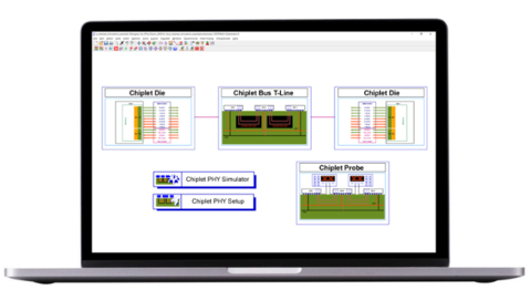
Chiplet PHY Designer provides engineers with an intuitive and integrated chiplet system analysis environment. (Photo: Business Wire)
As AI and data center chips grow more complex, ensuring reliable communication between chiplets becomes crucial for performance. The industry is addressing this challenge through open, emerging standards like UCIe and BoW that define the interconnects between chiplets within an advanced 2.5D/3D package. By adopting these standards and verifying chiplets for compliance, designers contribute to the growing ecosystem for chiplet interoperability, reducing costs and risks in semiconductor development.
Key Benefits of the Chiplet PHY Designer 2025:
- Ensures Interoperability: Verifies designs meet UCIe 2.0 and BoW standards, enabling seamless integration across advanced packaging ecosystems.
- Accelerates Time-to-Market: Automates simulation and compliance testing setup, such as Voltage Transfer Function (VTF), simplifying chiplet design workflows.
- Improves Design Accuracy: Provides insight into signal integrity, bit error rate (BER), and crosstalk analysis, reducing risks of costly silicon re-spins.
- Optimizes Clocking Designs: Supports advanced clocking scheme analysis, such as quarter-rate data rate (QDR), for precise synchronization in high-speed interconnects.
Hee-Soo Lee, High-Speed Digital Segment Lead, Keysight EDA, said: “Keysight EDA launched Chiplet PHY Designer one year ago as the industry’s first pre-silicon validation tool to provide in-depth modeling and simulation capabilities; this enabled chiplet designers to rapidly and accurately verify that their designs meet specifications before tapeout. The latest release keeps pace with evolving standards like UCIe 2.0 and BoW while delivering new features, such as the QDR clocking scheme and systematic crosstalk analysis for single-ended buses. Engineers using Chiplet PHY Designer save time and avoid costly rework, ensuring their designs meet performance requirements before manufacturing. Early adopters, like Alphawave Semi, attest that Chiplet PHY Designer ensures seamless operation and interoperability for 2.5D/3D solutions available to their chiplet customers.”
See Chiplet PHY Designer at DesignCon
Keysight will demonstrate Chiplet PHY Designer at its DesignCon booth, #1039, at the Santa Clara Convention Center from January 29 to 30, 2025.
Resources:
About Keysight Technologies
At Keysight (NYSE: KEYS), we inspire and empower innovators to bring world-changing technologies to life. As an S&P 500 company, we’re delivering market-leading design, emulation, and test solutions to help engineers develop and deploy faster, with less risk, throughout the entire product life cycle. We’re a global innovation partner enabling customers in communications, industrial automation, aerospace and defense, automotive, semiconductor, and general electronics markets to accelerate innovation to connect and secure the world. Learn more at Keysight Newsroom and www.keysight.com.
View source version on businesswire.com: https://www.businesswire.com/news/home/20250121466743/en/
Contacts
Keysight Media Contacts
North America PR Team
pdl-americas-keysight-pr@keysight.com
Fusako Dohi
Asia
+81 42 660-2162
fusako_dohi@keysight.com
Jenny Gallacher
Europe
+44 (0) 7800 737 982
jenny.gallacher@keysight.com
If you believe this article contains misleading, harmful, or spam content, please let us know.
Report this articleMore News
View More


Recent Quotes
View MoreQuotes delayed at least 20 minutes.
By accessing this page, you agree to the Privacy Policy and Terms Of Service.