Bruker Experiences Growth in Semiconductor Advanced Packaging Market Fueled by AI Demands
Bruker Corporation (Nasdaq: BRKR) today announced the shipment and installation of the 15th InSight WLI 3D optical metrology system to a leading semiconductor manufacturer. The installation is part of a larger order from this semiconductor manufacturer for 27 Bruker optical metrology systems in 2025. This reflects the growing demand for high-performance metrology that can support advanced packaging requirements in the latest generation AI high-performance chip manufacturing processes.
This press release features multimedia. View the full release here: https://www.businesswire.com/news/home/20250624897472/en/
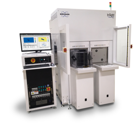
Bruker InSight WLI 3D optical metrology systems measure key manufacturing process steps that enable the production of advanced AI chips.
As artificial intelligence becomes increasingly embedded in consumer and industrial technologies, the chips powering these systems must deliver higher performance, faster data processing, and greater energy efficiency. To meet these demands, semiconductor manufacturers are turning to advanced packaging—a transformative approach that enables the integration of multiple chips into a single, compact package. Unlike traditional electronics packaging, advanced packaging supports multi-die stacking and heterogeneous integration, combining chips for processors, memory, and accelerators into unified systems. This architecture is essential for AI workloads, which require high bandwidth, low latency, and power efficiency, but it also introduces new manufacturing challenges in precision alignment and structural integrity. These challenges make Bruker’s advanced metrology solutions critical to ensuring performance and reliability.
“For decades, Bruker has partnered closely with semiconductor manufacturers to develop metrology solutions that meet the industry's aggressive roadmap needs,” said David V. Rossi, President of Bruker Nano Surfaces and Metrology Division. “This recent multi-system advanced packaging metrology order affirms how integral Bruker’s metrology is to the semiconductor industry’s technological leaps, such as the shift to advanced packaging for AI chip manufacturing.”
Bruker’s InSight WLI system is specifically designed for advanced packaging measurement requirements, providing non-contact, high-resolution 3D optical metrology that accurately measures layer-to-layer alignment, surface topography, and coplanarity—all capabilities that are essential for maintaining yield and quality. As new fabrication facilities continue to come online, Bruker anticipates further demand for their suite of advanced semiconductor metrology systems.
About Bruker Corporation – Leader of the Post-Genomic Era
Bruker is enabling scientists and engineers to make breakthrough post-genomic discoveries and develop new applications that improve the quality of human life. Bruker’s high performance scientific instruments and high value analytical and diagnostic solutions enable scientists to explore life and materials at molecular, cellular, and microscopic levels. In close cooperation with our customers, Bruker is enabling innovation, improved productivity, and customer success in post-genomic life science molecular and cell biology research, in applied and biopharma applications, in microscopy and nanoanalysis, as well as in industrial and cleantech research, and next-gen semiconductor metrology in support of AI. Bruker offers differentiated, high-value life science and diagnostics systems and solutions in preclinical imaging, clinical phenomics research, proteomics and multiomics, spatial and single-cell biology, functional structural and condensate biology, as well as in clinical microbiology and molecular diagnostics. For more information, please visit www.bruker.com.
View source version on businesswire.com: https://www.businesswire.com/news/home/20250624897472/en/
Contacts
Investor Contact:
Joe Kostka
Director, Investor Relations
Bruker Corporation
T: +1 (978) 313-5800
E: Investor.Relations@bruker.com
More News
View More


Recent Quotes
View More
Quotes delayed at least 20 minutes.
By accessing this page, you agree to the Privacy Policy and Terms Of Service.