Forge Nano Triples Semiconductor ALD Tool Production Space with New State-of-the-Art Cleanroom to Accommodate Growing Demand for Commercial Wafer Coating Equipment
- 2,000 sq/ft cleanroom dedicated to manufacturing commercial ALD equipment for 200mm semiconductor markets
- TEPHRA™ ALD cluster tools expected for customer delivery in early 2025
- Forge Nano plans customer TEPHRA™ demonstration, facility tour
DENVER, Jan. 29, 2025 (GLOBE NEWSWIRE) -- Forge Nano, Inc., an atomic layer deposition solution provider, today announced the completion of its new semiconductor cleanroom. The 2,000 sq/ft cleanroom enables Forge Nano to manufacture multiple commercial TEPHRA™ ALD cluster tools to accommodate growing equipment demand from the semiconductor market.
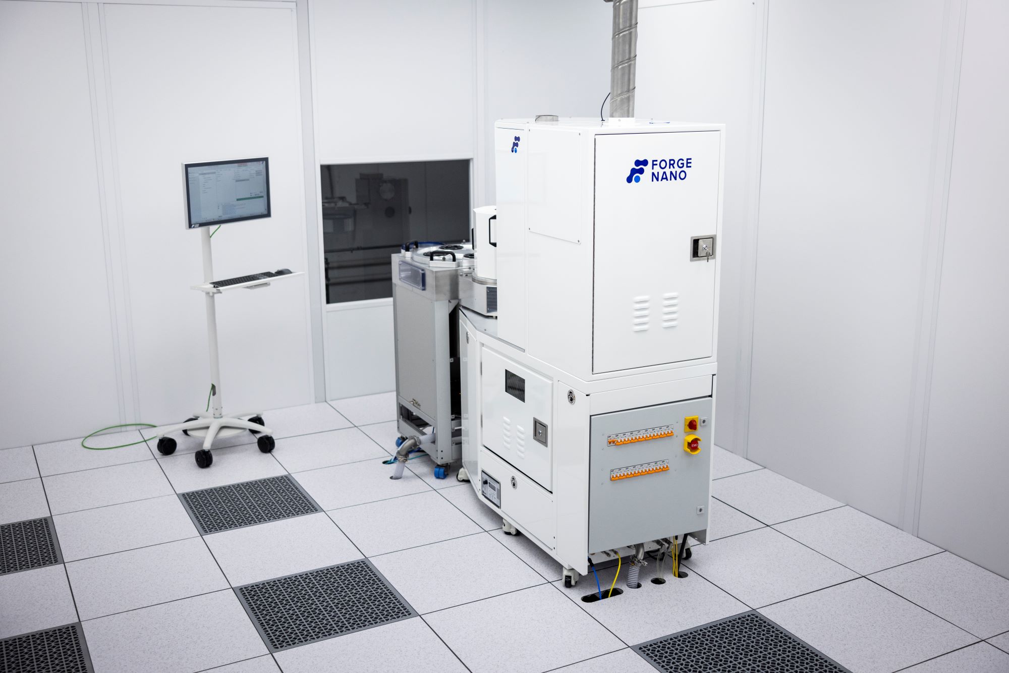
Forge Nano TEPHRA ALD cluster tool in the new cleanroom production space
Forge Nano announced the expansion of its semiconductor ALD business in 2024 with the launch of TEPHRA. Forge Nano’s ability to coat single wafers at 10x the throughput of traditional ALD systems has significantly grown customer demand thus requiring an expansion of the Company’s manufacturing capacity.
“The Forge Nano TEPHRA can enable conformal metal barrier seed layers for through silicon and through glass vias at aspect ratios greater than 25:1 at production speeds,” said Matt Weimer, Director of R&D at Forge Nano. “With this new cleanroom, Forge Nano will be able to showcase the capabilities of our ALDx atomic layer deposition processes to our customers and further our solutions for advanced packaging and 3D chip integration.”
The new cleanroom provides a Class 10 (ISO 4) space for processing sensitive customer samples and includes a metrology lab for advanced thin-film measurement and particle inspection. The remainder of the cleanroom will house Forge Nano’s own internal TEPHRA tool and provide space to build multiple customer tools, serving as a dual operating space for demonstrations and manufacturing. In addition to increased manufacturing space, this expansion is poised to accelerate Forge Nano’s ability to provide proof-of-concept and commercial solution validation to manufacturers planning to integrate new ALD processes.
Powered by Forge Nano’s ALDx technology, which offers ultrathin, uniform, pinhole-free films with an unprecedented 10x throughput for single-wafer processing, TEPHRA is dedicated to the manufacturing of specialty semiconductor applications on 200mm wafers and below. With efficient chemical use, rapid cycle times, increased yield, and low-risk manufacturing, TEPHRA is the only single-wafer cluster tool with commercial throughput speeds serving 200mm applications in advanced packaging, power semiconductor, radio frequency devices (RFD), microLEDs, microelectromechanical systems (MEMS), and more.
Forge Nano expects to deliver TEPHRA tools in early 2025. Forge Nano is offering on-site TEPHRA demonstrations to new and existing customers starting in early 2025. For more details on how to participate in the upcoming demonstration, please visit: https://www.forgenano.com/semiconductors
For more information on Forge Nano’s TEPHRA product, visit the TEPHRA product page at: https://www.forgenano.com/products/tephra
About Forge Nano
Forge Nano is designing the future of material change. With proprietary ALDx technology, Forge Nano enables semiconductor fabs to conformally coat 200mm wafers for encapsulation, passivation, high-κ dielectric and metal barrier seed applications. Forge Nano’s team of scientists have worked with an expansive portfolio of commercial partners to develop custom solutions to meet any need at any scale, from small-scale R&D and laboratory work to large-scale, high-volume production. Learn more at https://www.forgenano.com
Contact
Will McKenna
Brand Communications Director for Forge Nano
wmckenna@forgenano.com
(720) 432-6669
A photo accompanying this announcement is available at https://www.globenewswire.com/NewsRoom/AttachmentNg/b8df4162-ad95-4859-a64c-ab66fd9ae3b3

![]()
More News
View More


Recent Quotes
View MoreQuotes delayed at least 20 minutes.
By accessing this page, you agree to the Privacy Policy and Terms Of Service.