Hitachi High-Tech Launches High-Throughput and High-Sensitivity Wafer Surface Inspection System LS9600
By:
Hitachi, Ltd. via
JCN Newswire
December 13, 2022 at 06:14 AM EST

TOKYO, Dec 13, 2022 - (JCN Newswire) - Hitachi High-Tech Corporation announced today the launch of the LS9600, a new system for detecting particles and defects on non-patterned wafer surfaces. It features a new high-output, short-wavelength laser that improves throughput at the sensitivity levels required for the mass production of cutting-edge semiconductor devices by approx. 2.6 times compared to our previous generation systems. By introducing this product, Hitachi High-Tech will continue to help to improve yields and reduce inspection costs associated with customers' mass production of semiconductor devices.
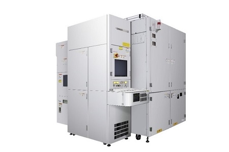 |
| Wafer Surface Inspection System LS9600 |
Development Background
Non-patterned wafer inspection systems are used for applications such as controlling the condition (cleanliness) of non-patterned wafers to manage particles and defects in semiconductor device manufacturing equipment. Due to the shrinking of semiconductor devices, the defects of interest (DOIs), which impact yield during the manufacturing process, have also become smaller in size. As a result, there is a growing need for high-sensitivity inspection that can detect DOIs of 20 nm and smaller across the entire surface of non-patterned wafers. In addition to high-sensitivity inspection to improve yield, there is also a strong demand for high throughput, which leads to lower inspection costs.
Key New Technologies
This system achieves both high sensitivity and high throughput by implementing the following new technologies.
1. High-Output, Short-Wavelength Laser
The deep-ultraviolet laser has a higher output and shorter wavelength than legacy systems, which increases the amount of light scattered by microscopic defects, thereby achieving a higher degree of sensitivity.
2. New Optical Detection System
The new optical detection system features a larger surface area to capture light scattered by DOIs compared to the legacy systems. In addition, its newly developed high-sensitivity sensor has improved the detection rate of weak scattered light by around 20%.
3. New Data Processing System
Improved scattered light data-processing algorithms deliver higher sensitivity, together with higher throughput due to high-speed, real-time data processing.
By using this product, as well as our wafer optical inspection systems, and electron beam-based products such as a traditional CD-SEM(1) and DR-SEM(2), Hitachi High-Tech is working to meet customers' various needs in processing, measurement, and inspection throughout the semiconductor manufacturing process. We will continue to provide innovative and digitally enhanced solutions to our products for the upcoming technology challenges, and create new value together with our customers, as well as contributing to cutting-edge manufacturing.
(1) CD-SEM (Critical Dimension-Scanning Electron Microscope): An equipment for measuring the microscopic circuit patterns on semiconductor wafers. Used for inspections on semiconductor devices development and production lines, these systems are essential for yield management.
(2) DR-SEM (Defect Review-Scanning Electron Microscope): An equipment for reviewing the microscopic circuit patterns and defects on semiconductor wafers. Used for inspections on semiconductor devices development and production lines, these systems are essential for yield management.
About Hitachi High-Tech
Hitachi High-Tech, headquartered in Tokyo, Japan, is engaged in activities in a broad range of fields, including manufacture and sales of clinical analyzers, biotechnology products, and analytical instruments, semiconductor manufacturing equipment and analysis equipment. and providing high value-added solutions in fields of social & industrial infrastructures and mobility, etc. The company's consolidated revenues for FY 2021 were approx. JPY 576.8 billion [USD 5.1 billion]. For further information, visit www.hitachi-hightech.com/global/
Contact:
Yuuki Minatani
Business Planning Dept., Metrology Systems Div.,
Nano-Technology Solution Business Group, Hitachi High-Tech Corporation
E-mail: yuki.minatani.dc@hitachi-hightech.com
Source: Hitachi, Ltd.
Copyright 2022 JCN Newswire . All rights reserved.
More News
View More
3 Stocks to Buy for the Evolution of AI Infrastructure ↗
Today 8:39 EST
How Semtech’s Data Center Chips Are Powering the AI Boom ↗
Today 7:25 EST
Keysight Technologies' Surge: The Market Wakes Up to This AI Play ↗
November 27, 2025

Is American Express the Credit Stock For a K-Shaped Economy? ↗
November 27, 2025
Via MarketBeat

Powering Up: How a Credit Upgrade Fuels Vistra’s AI Ambitions ↗
November 27, 2025
Recent Quotes
View More
Stock Quote API & Stock News API supplied by www.cloudquote.io
Quotes delayed at least 20 minutes.
By accessing this page, you agree to the Privacy Policy and Terms Of Service.
Quotes delayed at least 20 minutes.
By accessing this page, you agree to the Privacy Policy and Terms Of Service.
© 2025 FinancialContent. All rights reserved.
>