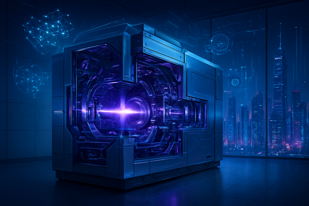
In a development that has sent shockwaves through the global semiconductor industry and the halls of power in Washington, reports have emerged of a functional Extreme Ultraviolet (EUV) lithography prototype operating within a high-security facility in Shenzhen. This breakthrough, described by industry insiders as China’s "Manhattan Project" for chips, represents the first credible evidence that Beijing has successfully bypassed the stringent export controls led by the United States and the Netherlands. The machine, which uses a novel light source and domestic optics, marks a definitive end to the era where EUV technology was the exclusive domain of a single Western-aligned company.
The immediate significance of this achievement cannot be overstated. For years, the inability to acquire EUV tools from ASML (NASDAQ: ASML) was considered the "Great Wall" preventing China from advancing to 5nm and 3nm process nodes. By successfully generating a stable EUV beam and integrating it with a domestic lithography system, Chinese engineers have effectively neutralized the most potent weapon in the Western technological blockade. This development signals that China is no longer merely reacting to sanctions but is actively architecting a parallel, sovereign semiconductor ecosystem that is immune to foreign interference.
Technical Defiance: LDP and the SSMB Alternative
The Shenzhen prototype, while functional, represents a radical departure from the architecture pioneered by ASML. While ASML’s machines utilize Laser-Produced Plasma (LPP)—a process involving firing high-power lasers at microscopic tin droplets—the Chinese system reportedly employs Laser-Induced Discharge Plasma (LDP). This method vaporizes tin between electrodes via high-voltage discharge, a simpler and more cost-effective approach that avoids some of the complex laser-timing patents held by ASML and its U.S. partner, Cymer. While the current LDP output is estimated at 50–100W—significantly lower than ASML’s 250W+ commercial standard—it is sufficient for the trial production of 5nm-class chips.
Furthermore, the breakthrough is supported by a secondary, even more ambitious light source project led by Tsinghua University. This involves Steady-State Micro-Bunching (SSMB), which utilizes a particle accelerator to generate a "clean" EUV beam. If successfully scaled, SSMB could potentially reach power levels exceeding 1kW, far surpassing current Western capabilities and eliminating the debris issues associated with tin-plasma systems. On the optics front, the Changchun Institute of Optics, Fine Mechanics and Physics (CIOMP) has reportedly achieved 65% reflectivity with domestic molybdenum-silicon multi-layer mirrors, a feat previously thought to be years away for Chinese material science.
Unlike the compact, "school bus-sized" machines produced in Veldhoven, the Shenzhen prototype is described as a "behemoth" that occupies nearly an entire factory floor. This massive scale was a necessary engineering trade-off to accommodate less refined domestic components and to provide the stabilization required for the LDP light source. Despite its size, the precision is reportedly world-class; the system utilizes a domestic "alignment interferometer" to position mirrors with sub-nanometer accuracy, mimicking the legendary precision of Germany’s Carl Zeiss.
The reaction from the international research community has been one of stunned disbelief. Researchers at Taiwan Semiconductor Manufacturing Co. (NYSE: TSM), commonly known as TSMC, have privately characterized the LDP breakthrough as a "DeepSeek moment for lithography," referring to the sudden and unexpected leap in capability. While some experts remain skeptical about the machine’s "uptime" and commercial yield, the consensus is that the fundamental physics of the "EUV bottleneck" have been solved by Chinese scientists.
Market Disruption: The End of the ASML Monopoly
The emergence of a domestic Chinese EUV tool poses an existential threat to the current market hierarchy. ASML (NASDAQ: ASML), which has enjoyed a 100% market share in EUV lithography, saw its stock price dip as the news of the Shenzhen prototype solidified. While ASML’s current High-NA EUV machines remain the gold standard for efficiency, the existence of a "good enough" Chinese alternative removes the leverage the West once held over China’s primary foundry, SMIC (HKG: 0981). SMIC is already reportedly integrating these domestic tools into its "Project Dragon" production lines, aiming for 5nm-class trial production by the end of 2025.
Huawei, acting as the central coordinator and primary financier of the project, stands as the biggest beneficiary. By securing a domestic supply of advanced chips, Huawei can finally reclaim its position in the high-end smartphone and AI server markets without fear of further US Department of Commerce restrictions. Other Shenzhen-based companies, such as SiCarrier and Shenzhen Xin Kailai, have also emerged as critical "shadow" suppliers, providing the metrology and wafer-handling subsystems that were previously sourced from companies like Nikon (TYO: 7731) and Canon (TYO: 7751).
The competitive implications for Western tech giants are severe. If China can mass-produce 5nm chips using domestic EUV, the cost of AI hardware and high-performance computing in the mainland will plummet, giving Chinese AI firms a significant cost advantage over global rivals who must pay a premium for Western-regulated silicon. This could lead to a bifurcation of the global tech market, with a "Western Stack" led by Nvidia (NASDAQ: NVDA) and TSMC, and a "China Stack" powered by Huawei and SMIC.
Geopolitical Fallout and the Global AI Landscape
This breakthrough fits into a broader trend of "technological decoupling" that has accelerated throughout 2025. The US government has already responded with alarm; reports indicate the Commerce Department is moving to revoke export waivers for TSMC’s Nanjing plant and Samsung’s (KRX: 005930) Chinese facilities in a desperate bid to slow the integration of domestic tools. However, many analysts argue that these "scorched earth" policies may have come too late. The Shenzhen breakthrough proves that heavy-handed export controls can act as a catalyst for innovation, forcing a nation to achieve in five years what might have otherwise taken fifteen.
The wider significance for the AI landscape is profound. Advanced AI models require massive clusters of high-performance GPUs, which in turn require the advanced nodes that only EUV can provide. By breaking the EUV barrier, China has secured its seat at the table for the future of General Artificial Intelligence (AGI). There are, however, significant concerns regarding the lack of international oversight. A completely domestic, opaque semiconductor supply chain in China could lead to the rapid proliferation of advanced dual-use technologies with military applications, further straining the fragile "AI safety" consensus between the US and China.
Comparatively, this milestone is being viewed with the same historical weight as the launch of Sputnik or the first successful test of a domestic Chinese nuclear weapon. It marks the transition of China from a "fast follower" in the semiconductor industry to a peer competitor capable of original, high-stakes fundamental research. The era of Western "choke points" is effectively over, replaced by a new, more dangerous era of "parallel breakthroughs."
The Road Ahead: Scaling and Commercialization
Looking toward 2026 and beyond, the primary challenge for the Shenzhen project is scaling. Moving from a single, factory-floor-sized prototype to a fleet of reliable, high-yield production machines is a monumental task. Experts predict that China will spend the next 24 months focusing on "yield optimization"—reducing the error rates in the lithography process and increasing the power of the LDP light source to improve throughput. If these hurdles are cleared, we could see the first commercially available Chinese 5nm chips hitting the market by 2027.
The next frontier will be the transition from LDP to the aforementioned SSMB technology. If the Tsinghua University particle accelerator project reaches maturity, it could allow China to leapfrog ASML’s current technology entirely. Predictive models from industry analysts suggest that by 2030, China could potentially lead the world in "Clean EUV" production, offering a more sustainable and higher-power alternative to the tin-based systems currently used by the rest of the world.
However, challenges remain. The recruitment of former ASML and Zeiss engineers—often under aliases and with massive signing bonuses—has created a "talent war" that could lead to further legal and diplomatic skirmishes. Furthermore, the massive energy requirements of the Shenzhen "behemoth" machine mean that China will need to build dedicated power infrastructure for its new generation of "Giga-fabs."
A New Era of Semiconductor Sovereignty
The secret EUV breakthrough in Shenzhen represents a watershed moment in the history of technology. It is the clearest sign yet that the global order of the 21st century will be defined by technological sovereignty rather than globalized supply chains. By overcoming the most complex engineering challenge in human history—manipulating light at the extreme ultraviolet spectrum to print billions of transistors on a sliver of silicon—China has declared its independence from the Western tech ecosystem.
In the coming weeks, the world will be watching for the official response from the Dutch government and the potential for new, even more restrictive measures from the United States. However, the genie is out of the bottle. The "Shenzhen Prototype" is no longer a rumor; it is a functioning reality that has redrawn the map of global power. As we move into 2026, the focus will shift from if China can make advanced chips to how many they can make, and what that means for the future of global AI supremacy.
This content is intended for informational purposes only and represents analysis of current AI and semiconductor developments.
TokenRing AI delivers enterprise-grade solutions for multi-agent AI workflow orchestration, AI-powered development tools, and seamless remote collaboration platforms.
For more information, visit https://www.tokenring.ai/.