The semiconductor industry is undergoing a profound transformation, driven by the escalating demands of Artificial Intelligence (AI) for unprecedented computational power, speed, and efficiency. At the heart of this revolution are advancements in chip packaging and the emergence of chiplet technology, which together are extending performance scaling beyond traditional transistor miniaturization. These innovations are not merely incremental improvements but represent a foundational shift that is redefining how computing systems are built and optimized for the AI era, with significant implications for the tech landscape as of October 2025.
This critical juncture is characterized by a rapid evolution in chip packaging technologies and the widespread adoption of chiplet architectures, collectively pushing the boundaries of performance scaling beyond traditional transistor miniaturization. This shift is enabling the creation of more powerful, efficient, and specialized AI hardware, directly addressing the limitations of traditional monolithic chip designs and the slowing of Moore's Law.
Technical Foundations of the AI Hardware Revolution
The advancements driving this new era of silicon are multifaceted, encompassing sophisticated packaging techniques, groundbreaking lithography systems, and a paradigm shift in chip design.
Nikon's DSP-100 Digital Lithography System: Precision for Advanced Packaging
Nikon has introduced a pivotal tool for advanced packaging with its Digital Lithography System DSP-100. Orders for this system commenced in July 2025, with a scheduled release in Nikon's (TYO: 7731) fiscal year 2026. The DSP-100 is specifically designed for back-end semiconductor manufacturing processes, supporting next-generation chiplet integrations and heterogeneous packaging applications with unparalleled precision and scalability.
A standout feature is its maskless technology, which utilizes a spatial light modulator (SLM) to directly project circuit patterns onto substrates. This eliminates the need for photomasks, thereby reducing production costs, shortening development times, and streamlining the manufacturing process. The system supports large square substrates up to 600x600mm, a significant advancement over the limitations of 300mm wafers. For 100mm-square packages, the DSP-100 can achieve up to nine times higher productivity per substrate compared to using 300mm wafers, processing up to 50 panels per hour. It delivers a high resolution of 1.0μm Line/Space (L/S) and excellent overlay accuracy of ≤±0.3μm, crucial for the increasingly fine circuit patterns in advanced packages. This innovation directly addresses the rising demand for high-performance AI devices in data centers by enabling more efficient and cost-effective advanced packaging.
It is important to clarify that while Nikon has a history of extensive research in Extreme Ultraviolet (EUV) lithography, it is not a current commercial provider of EUV systems for leading-edge chip fabrication. The DSP-100 focuses on advanced packaging rather than the sub-3nm patterning of individual chiplets themselves, a domain largely dominated by ASML (AMS: ASML).
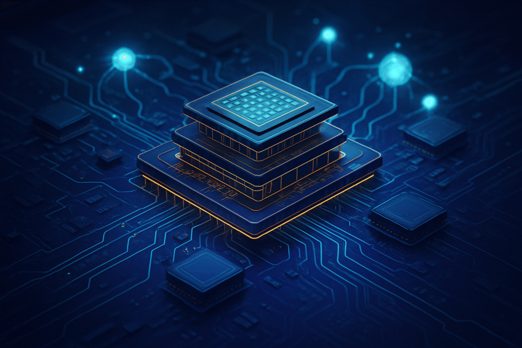
Chiplet Technology: Modular Design for Unprecedented Performance
Chiplet technology represents a paradigm shift from monolithic chip design, where all functionalities are integrated onto a single large die, to a modular "lego-block" approach. Small, specialized integrated circuits (ICs), or chiplets, perform specific tasks (e.g., compute, memory, I/O, AI accelerators) and are interconnected within a single package.
This modularity offers several architectural benefits over monolithic designs:
- Improved Yield and Cost Efficiency: Manufacturing smaller chiplets significantly increases the likelihood of producing defect-free dies, boosting overall yield and allowing for the selective use of expensive advanced process nodes only for critical components.
- Enhanced Performance and Power Efficiency: By allowing each chiplet to be designed and fabricated with the most suitable process technology for its specific function, overall system performance can be optimized. Close proximity of chiplets within advanced packages, facilitated by high-bandwidth and low-latency interconnects, dramatically reduces signal travel time and power consumption.
- Greater Scalability and Customization: Designers can mix and match chiplets to create highly customized solutions tailored for diverse AI applications, from high-performance computing (HPC) to edge AI, and for handling the escalating complexity of large language models (LLMs).
- Reduced Time-to-Market: Reusing validated chiplets across multiple products or generations drastically cuts down development cycles.
- Overcoming Reticle Limits: Chiplets effectively circumvent the physical size limitations (reticle limits) inherent in manufacturing monolithic dies.
Advanced Packaging Techniques: The Glue for Chiplets
Advanced packaging techniques are indispensable for the effective integration of chiplets, providing the necessary high-density interconnections, efficient power delivery, and robust thermal management required for high-performance AI systems.
- 2.5D Packaging: In this approach, multiple components, such as CPU/GPU dies and High-Bandwidth Memory (HBM) stacks, are placed side-by-side on a silicon or organic interposer. This technique dramatically increases bandwidth and reduces latency between components, crucial for AI workloads.
- 3D Packaging: This involves vertically stacking active dies, leading to even greater integration density. 3D packaging directly addresses the "memory wall" problem by enabling significantly higher bandwidth between processing units and memory through technologies like Through-Silicon Vias (TSVs), which provide high-density vertical electrical connections.
- Hybrid Bonding: A cutting-edge 3D packaging technique that facilitates direct copper-to-copper (Cu-Cu) connections at the wafer level. This method achieves ultra-fine interconnect pitches, often in the single-digit micrometer range, and supports bandwidths up to 1000 GB/s while maintaining high energy efficiency. Hybrid bonding is a key enabler for the tightly integrated, high-performance systems crucial for modern AI.
- Fan-Out Packaging (FOPLP/FOWLP): These techniques eliminate the need for traditional package substrates by embedding the dies directly into a molding compound, allowing for more I/O connections in a smaller footprint. Fan-out panel-level packaging (FOPLP) is a significant trend, supporting larger substrates than traditional wafer-level packaging and offering superior production efficiency.
The semiconductor industry and AI community have reacted very positively to these advancements, recognizing them as critical enablers for developing high-performance, power-efficient, and scalable computing systems, especially for the massive computational demands of AI workloads.
Competitive Landscape and Corporate Strategies
The shift to advanced packaging and chiplet technology has profound competitive implications, reshaping the market positioning of tech giants and creating significant opportunities for others. As of October 2025, companies with strong ties to leading foundries and early access to advanced packaging capacities hold a strategic advantage.
NVIDIA (NASDAQ: NVDA) is a primary beneficiary and driver of advanced packaging demand, particularly for its AI accelerators. Its H100 GPU, for instance, leverages 2.5D CoWoS (Chip-on-Wafer-on-Substrate) packaging to integrate a powerful GPU and six HBM stacks. NVIDIA CEO Jensen Huang emphasizes advanced packaging as critical for semiconductor innovation. Notably, NVIDIA is reportedly investing $5 billion in Intel's advanced packaging services, signaling packaging's new role as a competitive edge and providing crucial second-source capacity.
Intel (NASDAQ: INTC) is heavily invested in chiplet technology through its IDM 2.0 strategy and advanced packaging technologies like Foveros (3D stacking) and EMIB (Embedded Multi-die Interconnect Bridge, a 2.5D solution). Intel is deploying multiple "tiles" (chiplets) in its Meteor Lake and upcoming Arrow Lake processors, allowing for CPU, GPU, and AI performance scaling. Intel Foundry Services (IFS) offers these advanced packaging services to external customers, positioning Intel as a key player. Microsoft (NASDAQ: MSFT) has commissioned Intel to manufacture custom AI accelerator and data center chips using its 18A process technology and "system-level foundry" strategy.
AMD (NASDAQ: AMD) has been a pioneer in chiplet architecture adoption. Its Ryzen and EPYC processors extensively use chiplets, and its Instinct MI300 series (MI300A for AI/HPC accelerators) integrates GPU, CPU, and memory chiplets in a single package using advanced 2.5D and 3D packaging techniques, including hybrid bonding for 3D V-Cache. This approach provides high throughput, scalability, and energy efficiency, offering a competitive alternative to NVIDIA.
TSMC (TPE: 2330 / NYSE: TSM), the world's largest contract chipmaker, is fortifying its indispensable role as the foundational enabler for the global AI hardware ecosystem. TSMC is heavily investing in expanding its advanced packaging capacity, particularly for CoWoS and SoIC (System on Integrated Chips), to meet the "very strong" demand for HPC and AI chips. Its expanded capacity is expected to ease the CoWoS crunch and enable the rapid deployment of next-generation AI chips.
Samsung (KRX: 005930) is actively developing and expanding its advanced packaging solutions to compete with TSMC and Intel. Through its SAINT (Samsung Advanced Interconnection Technology) program and offerings like I-Cube (2.5D packaging) and X-Cube (3D IC packaging), Samsung aims to merge memory and processors in significantly smaller sizes. Samsung Foundry recently partnered with Arm (NASDAQ: ARM), ADTechnology, and Rebellions to develop an AI CPU chiplet platform for data centers.
ASML (AMS: ASML), while not directly involved in packaging, plays a critical indirect role. Its advanced lithography tools, particularly its High-NA EUV technology, are essential for manufacturing the leading-edge wafers and interposers that form the basis of advanced packaging and chiplets.
AI Companies and Startups also stand to benefit. Tech giants like Google (NASDAQ: GOOGL), Amazon (NASDAQ: AMZN), and Microsoft are heavily reliant on advanced packaging and chiplets for their custom AI chips and data center infrastructure. Chiplet technology enables smaller AI startups to leverage pre-designed components, reducing R&D time and costs, and fostering innovation by lowering the barrier to entry for specialized AI hardware development.
The industry is moving away from traditional monolithic chip designs towards modular chiplet architectures, addressing the physical and economic limits of Moore's Law. Advanced packaging has become a strategic differentiator and a new battleground for competitive advantage, with securing innovation and capacity in packaging now as crucial as breakthroughs in silicon design.
Wider Significance and AI Landscape Impact
These advancements in chip packaging and chiplet technology are not merely technical feats; they are fundamental to addressing the "insatiable demand" for scalable AI infrastructure and are reshaping the broader AI landscape.
Fit into Broader AI Landscape and Trends:
AI workloads, especially large generative language models, require immense computational resources, vast memory bandwidth, and high-speed interconnects. Advanced packaging (2.5D/3D) and chiplets are critical for building powerful AI accelerators (GPUs, ASICs, NPUs) that can handle these demands by integrating multiple compute cores, memory interfaces, and specialized AI accelerators into a single package. For data center infrastructure, these technologies enable custom silicon solutions to affordably scale AI performance, manage power consumption, and address the "memory wall" problem by dramatically increasing bandwidth between processing units and memory. Innovations like co-packaged optics (CPO), which integrate optical I/O directly to the AI accelerator interface using advanced packaging, are replacing traditional copper interconnects to reduce power and latency in multi-rack AI clusters.
Impacts on Performance, Power, and Cost:
- Performance: Advanced packaging and chiplets lead to optimized performance by enabling higher interconnect density, shorter signal paths, reduced electrical resistance, and significantly increased memory bandwidth. This results in faster data transfer, lower latency, and higher throughput, crucial for AI applications.
- Power: These technologies contribute to substantial power efficiency gains. By optimizing the layout and interconnection of components, reducing interconnect lengths, and improving memory hierarchies, advanced packages can lower energy consumption. Chiplet-based approaches can lead to 30-40% lower energy consumption for the same workload compared to monolithic designs, translating into significant savings for data centers.
- Cost: While advanced packaging itself can involve complex processes, it ultimately offers cost advantages. Chiplets improve manufacturing yields by allowing smaller dies, and heterogeneous integration enables the use of more cost-optimal manufacturing nodes for different components. Panel-level packaging with systems like Nikon's DSP-100 can further reduce production costs through higher productivity and maskless technology.
Potential Concerns:
- Complexity: The integration of multiple chiplets and the intricate nature of 2.5D/3D stacking introduce significant design and manufacturing complexity, including challenges in yield management, interconnect optimization, and especially thermal management due to increased function density.
- Standardization: A major hurdle for realizing a truly open chiplet ecosystem is the lack of universal standards. While initiatives like the Universal Chiplet Interconnect Express (UCIe) aim to foster interoperability between chiplets from different vendors, proprietary die-to-die interconnects still exist, complicating broader adoption.
- Supply Chain and Geopolitical Factors: Concentrating critical manufacturing capacity in specific regions raises geopolitical implications and concerns about supply chain disruptions.
Comparison to Previous AI Milestones:
These advancements, while often less visible than breakthroughs in AI algorithms or computing architectures, are equally fundamental to the current and future trajectory of AI. They represent a crucial engineering milestone that provides the physical infrastructure necessary to realize and deploy algorithmic and architectural breakthroughs at scale. Just as the development of GPUs revolutionized deep learning, chiplets extend this trend by enabling even finer-grained specialization, allowing for bespoke AI hardware. Unlike previous milestones primarily driven by increasing transistor density (Moore's Law), the current shift leverages advanced packaging and heterogeneous integration to achieve performance gains when silicon scaling limits are being approached. This redefines how computational power is achieved, moving from monolithic scaling to modular optimization.
The Road Ahead: Future Developments and Challenges
The future of chip packaging and chiplet technology is poised for transformative growth, driven by the escalating demands for higher performance, greater energy efficiency, and more specialized computing solutions.
Expected Near-Term (1-5 years) and Long-Term (Beyond 5 years) Developments:
In the near term, chiplet-based designs will see broader adoption beyond high-end CPUs and GPUs, extending to a wider range of processors. The Universal Chiplet Interconnect Express (UCIe) standard is expected to mature rapidly, fostering a more robust ecosystem for chiplet interoperability. Sophisticated heterogeneous integration, including the widespread adoption of 2.5D and 3D hybrid bonding, will become standard practice for high-performance AI and HPC systems. AI will increasingly play a role in optimizing chiplet-based semiconductor design.
Long-term, the industry is poised for fully modular semiconductor designs, with custom chiplets optimized for specific AI workloads dominating future architectures. The transition from 2.5D to more prevalent 3D heterogeneous computing will become commonplace. Further miniaturization, sustainable packaging, and integration with emerging technologies like quantum computing and photonics are also on the horizon.
Potential Applications and Use Cases:
The modularity, flexibility, and performance benefits of chiplets and advanced packaging are driving their adoption across a wide range of applications:
- High-Performance Computing (HPC) and Data Centers: Crucial for generative AI, machine learning, and AI accelerators, enabling unparalleled speed and energy efficiency.
- Consumer Electronics: Powering more powerful and efficient AI companions in smartphones, AR/VR devices, and wearables.
- Automotive: Essential for advanced autonomous vehicles, integrating high-speed sensors, real-time AI processing, and robust communication systems.
- Internet of Things (IoT) and Telecommunications: Enabling customized silicon for diverse IoT applications and vital for 5G and 6G networks.
Challenges That Need to Be Addressed:
Despite the immense potential, several significant challenges must be overcome for the widespread adoption of chiplets and advanced packaging:
- Standardization: The lack of a truly open chiplet marketplace due to proprietary die-to-die interconnects remains a major hurdle.
- Thermal Management: Densely packed multi-chiplet architectures create complex thermal management challenges, requiring advanced cooling solutions.
- Design Complexity: Integrating multiple chiplets requires advanced engineering, robust testing, and sophisticated Electronic Design Automation (EDA) tools.
- Testing and Validation: Ensuring the quality and reliability of chiplet-based systems is complex, requiring advancements in "known-good-die" (KGD) testing and system-level validation.
- Supply Chain Coordination: Ensuring the availability of compatible chiplets from different suppliers requires robust supply chain management.
Expert Predictions:
Experts are overwhelmingly positive, predicting chiplets will be found in almost all high-performance computing systems, crucial for reducing inter-chip communication power and achieving necessary memory bandwidth. They are seen as revolutionizing AI hardware by driving demand for specialized and efficient computing architectures, breaking the memory wall for generative AI, and accelerating innovation. The global chiplet market is experiencing remarkable growth, projected to reach hundreds of billions of dollars by the next decade. AI-driven design automation tools are expected to become indispensable for optimizing complex chiplet-based designs.
Comprehensive Wrap-Up and Future Outlook
The convergence of chiplets and advanced packaging technologies represents a "foundational shift" that will profoundly influence the trajectory of Artificial Intelligence. This pivotal moment in semiconductor history is characterized by a move from monolithic scaling to modular optimization, directly addressing the challenges of the "More than Moore" era.
Summary of Key Takeaways:
- Sustaining AI Innovation Beyond Moore's Law: Chiplets and advanced packaging provide an alternative pathway to performance gains, ensuring the rapid pace of AI innovation continues.
- Overcoming the "Memory Wall" Bottleneck: Advanced packaging, especially 2.5D and 3D stacking with HBM, dramatically increases bandwidth between processing units and memory, enabling AI accelerators to process information much faster and more efficiently.
- Enabling Specialized and Efficient AI Hardware: This modular approach allows for the integration of diverse, purpose-built processing units into a single, highly optimized package, crucial for developing powerful, energy-efficient chips demanded by today's complex AI models.
- Cost and Energy Efficiency: Chiplets and advanced packaging enable manufacturers to optimize cost by using the most suitable process technology for each component and improve energy efficiency by minimizing data travel distances.
Assessment of Significance in AI History:
This development echoes and, in some ways, surpasses the impact of previous hardware breakthroughs, redefining how computational power is achieved. It provides the physical infrastructure necessary to realize and deploy algorithmic and architectural breakthroughs at scale, solidifying the transition of AI from theoretical models to widespread practical applications.
Final Thoughts on Long-Term Impact:
Chiplet-based designs are poised to become the new standard for complex, high-performance computing systems, especially within the AI domain. This modularity will be critical for the continued scalability of AI, enabling the development of more powerful and efficient AI models previously thought unimaginable. The long-term impact will also include the widespread integration of co-packaged optics (CPO) and an increasing reliance on AI-driven design automation.
What to Watch for in the Coming Weeks and Months (October 2025 Context):
- Accelerated Adoption of 2.5D and 3D Hybrid Bonding: Expect to see increasingly widespread adoption of these advanced packaging technologies as standard practice for high-performance AI and HPC systems.
- Maturation of the Chiplet Ecosystem and Interconnect Standards: Watch for further standardization efforts, such as the Universal Chiplet Interconnect Express (UCIe), which are crucial for enabling seamless cross-vendor chiplet integration.
- Full Commercialization of HBM4 Memory: Anticipated in late 2025, HBM4 will provide another significant leap in memory bandwidth for AI accelerators.
- Nikon DSP-100 Initial Shipments: Following orders in July 2025, initial shipments of Nikon's DSP-100 digital lithography system are expected in fiscal year 2026. Its impact on increasing production efficiency for large-area advanced packaging will be closely monitored.
- Continued Investment and Geopolitical Dynamics: Expect aggressive and sustained investments from leading foundries and IDMs into advanced packaging capacity, often bolstered by government initiatives like the U.S. CHIPS Act.
- Increasing Role of AI in Packaging and Design: The industry is increasingly leveraging AI for improving yield management in multi-die assembly and optimizing EDA platforms.
- Emergence of New Materials and Architectures: Keep an eye on advancements in novel materials like glass-core substrates and the increasing integration of Co-Packaged Optics (CPO).
This content is intended for informational purposes only and represents analysis of current AI developments.
TokenRing AI delivers enterprise-grade solutions for multi-agent AI workflow orchestration, AI-powered development tools, and seamless remote collaboration platforms.
For more information, visit https://www.tokenring.ai/.