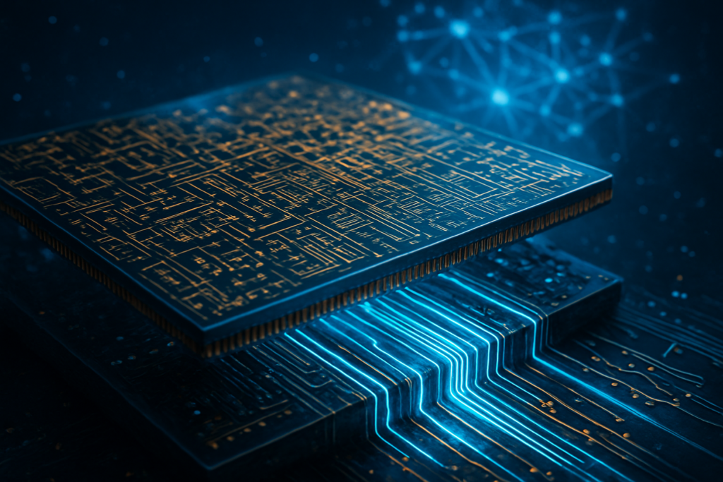
The semiconductor industry has reached a historic inflection point as the world’s leading chipmakers—Intel, TSMC, and Samsung—officially move power routing to the "backside" of the silicon wafer. This architectural shift, known as Backside Power Delivery Network (BSPDN), represents the most significant change to transistor design in over a decade. By relocating the complex web of power-delivery wires from the top of the chip to the bottom, manufacturers are finally decoupling power from signal, effectively "flipping" the traditional chip architecture to unlock unprecedented levels of efficiency and performance.
As of early 2026, this technology has transitioned from an experimental laboratory concept to the foundational engine of the AI revolution. With AI accelerators now pushing toward 1,000-watt power envelopes and consumer devices demanding more on-device intelligence than ever before, BSPDN has become the "lifeline" for the industry. Intel (NASDAQ: INTC) has taken an early lead with its PowerVia technology, while TSMC (NYSE: TSM) is preparing to counter with its more complex A16 process, setting the stage for a high-stakes battle over the future of high-performance computing.
For the past fifty years, chips have been built like a house where the plumbing and the electrical wiring are all crammed into the ceiling, competing for space with the occupants. In traditional "front-side" power delivery, both signal-carrying wires and power-delivery wires are layered on top of the transistors. As transistors have shrunk to the 2nm and 1.6nm scales, this "spaghetti" of wiring has become a massive bottleneck, causing signal interference and significant voltage drops (IR drop) that waste energy and generate heat.
Intel’s implementation, branded as PowerVia, solves this by using Nano-Through Silicon Vias (nTSVs) to route power directly from the back of the wafer to the transistors. This approach, debuted in the Intel 18A process, has already demonstrated a 30% reduction in voltage droop and a 15% improvement in performance-per-watt. By removing the power wires from the front side, Intel has also been able to pack transistors 30% more densely, as the signal wires no longer have to navigate around bulky power lines.
TSMC’s approach, known as Super PowerRail (SPR), which is slated for mass production in the second half of 2026 on its A16 node, takes the concept even further. While Intel uses nTSVs to reach the transistor layer, TSMC’s SPR connects the power network directly to the source and drain of the transistors. This "direct-contact" method is significantly more difficult to manufacture but promises even better electrical characteristics, including an 8–10% speed gain at the same voltage and up to a 20% reduction in power consumption compared to its standard 2nm process.
Initial reactions from the AI research community have been overwhelmingly positive. Experts at the 2026 International Solid-State Circuits Conference (ISSCC) noted that BSPDN effectively "resets the clock" on Moore’s Law. By thinning the silicon wafer to just a few micrometers to allow for backside routing, chipmakers have also inadvertently improved thermal management, as the heat-generating transistors are now physically closer to the cooling solutions on the back of the chip.
The shift to backside power delivery is creating a new hierarchy among tech giants. NVIDIA (NASDAQ: NVDA), the undisputed leader in AI hardware, is reportedly the anchor customer for TSMC’s A16 process. While their current "Rubin" architecture pushed the limits of front-side delivery, the upcoming "Feynman" architecture is expected to leverage Super PowerRail to maintain its lead in AI training. The ability to deliver more power with less heat is critical for NVIDIA as it seeks to scale its Blackwell successors into massive, multi-die "superchips."
Intel stands to benefit immensely from its first-mover advantage. By being the first to bring BSPDN to high-volume manufacturing with its 18A node, Intel has successfully attracted major foundry customers like Microsoft (NASDAQ: MSFT) and Amazon (NASDAQ: AMZN), both of which are designing custom AI silicon for their data centers. This "PowerVia-first" strategy has allowed Intel to position itself as a viable alternative to TSMC for the first time in years, potentially disrupting the existing foundry monopoly and shifting the balance of power in the semiconductor market.
Apple (NASDAQ: AAPL) and AMD (NASDAQ: AMD) are also navigating this transition with high stakes. Apple is currently utilizing TSMC’s 2nm (N2) node for the iPhone 18 Pro, but reports suggest they are eyeing A16 for their 2027 "M5" and "A20" chips to support more advanced generative AI features on-device. Meanwhile, AMD is leveraging its chiplet expertise to integrate backside power into its "Instinct" MI400 series, aiming to close the performance gap with NVIDIA by utilizing the superior density and clock speeds offered by the new architecture.
For startups and smaller AI labs, the arrival of BSPDN-enabled chips means more compute for every dollar spent on electricity. As power costs become the primary constraint for AI scaling, the 15-20% efficiency gains provided by backside power could be the difference between a viable business model and a failed venture. The competitive advantage will likely shift toward those who can most quickly adapt their software to take advantage of the higher clock speeds and increased core counts these new chips provide.
Beyond the technical specifications, backside power delivery represents a fundamental shift in the broader AI landscape. We are moving away from an era where "more transistors" was the only metric that mattered, into an era of "system-level optimization." BSPDN is not just about making transistors smaller; it is about making the entire system—from the power supply to the cooling unit—more efficient. This mirrors previous milestones like the introduction of FinFET transistors or Extreme Ultraviolet (EUV) lithography, both of which were necessary to keep the industry moving forward when physical limits were reached.
The environmental impact of this technology cannot be overstated. With data centers currently consuming an estimated 3-4% of global electricity—a figure projected to rise sharply due to AI demand—the efficiency gains from BSPDN are a critical component of the tech industry’s sustainability goals. A 20% reduction in power at the chip level translates to billions of kilowatt-hours saved across global AI clusters. However, this also raises concerns about "Jevons' Paradox," where increased efficiency leads to even greater demand, potentially offsetting the environmental benefits as companies simply build larger, more power-hungry models.
There are also significant geopolitical implications. The race to master backside power delivery has become a centerpiece of national industrial policies. The U.S. government’s support for Intel’s 18A progress and the Taiwanese government’s backing of TSMC’s A16 development highlight how critical this technology is for national security and economic competitiveness. Being the first to achieve high yields on BSPDN nodes is now seen as a marker of a nation’s technological sovereignty in the age of artificial intelligence.
Comparatively, the transition to backside power is being viewed as more disruptive than the move to 3D stacking (HBM). While HBM solved the "memory wall," BSPDN is solving the "power wall." Without it, the industry would have hit a hard ceiling where chips could no longer be cooled or powered effectively, regardless of how many transistors could be etched onto the silicon.
Looking ahead, the next two years will see the integration of backside power delivery with other emerging technologies. The most anticipated development is the combination of BSPDN with Complementary Field-Effect Transistors (CFETs). By stacking n-type and p-type transistors on top of each other and powering them from the back, experts predict another 50% jump in density by 2028. This would allow for smartphone-sized devices with the processing power of today’s high-end workstations.
In the near term, we can expect to see "backside signaling" experiments. Once the power is moved to the back, the front side of the chip is left entirely for signal routing. Researchers are already looking into moving some high-speed signal lines to the backside as well, which could further reduce latency and increase bandwidth for AI-to-AI communication. However, the primary challenge remains manufacturing yield. Thinning a wafer to the point where backside power is possible without destroying the delicate transistor structures is an incredibly precise process that will take years to perfect for mass production.
Experts predict that by 2030, front-side power delivery will be viewed as an antique relic of the "early silicon age." The future of AI silicon lies in "true 3D" integration, where power, signal, and cooling are interleaved throughout the chip structure. As we move toward the 1nm and sub-1nm eras, the innovations pioneered by Intel and TSMC today will become the standard blueprint for every chip on the planet, enabling the next generation of autonomous systems, real-time translation, and personalized AI assistants.
The shift to Backside Power Delivery marks the end of the "flat" era of semiconductor design. By moving the power grid to the back of the wafer, Intel and TSMC have broken through a physical barrier that threatened to stall the progress of artificial intelligence. The immediate results—higher clock speeds, better thermal management, and improved energy efficiency—are exactly what the industry needs to sustain the current pace of AI innovation.
As we move through 2026, the key metrics to watch will be the production yields of Intel’s 18A and the first samples of TSMC’s A16. While Intel currently holds the "first-to-market" crown, the long-term winner will be the company that can manufacture these complex architectures at the highest volume with the fewest defects. This transition is not just a technical upgrade; it is a total reimagining of the silicon chip that will define the capabilities of AI for the next decade.
In the coming weeks, keep an eye on the first independent benchmarks of Intel’s Panther Lake processors and any further announcements from NVIDIA regarding their Feynman architecture. The "Great Flip" has begun, and the world of computing will never look the same.
This content is intended for informational purposes only and represents analysis of current AI developments.
TokenRing AI delivers enterprise-grade solutions for multi-agent AI workflow orchestration, AI-powered development tools, and seamless remote collaboration platforms.
For more information, visit https://www.tokenring.ai/.