The world of semiconductor manufacturing has reached a historic inflection point. As of January 2026, the industry has officially moved beyond the constraints of traditional transistor scaling and entered the "Angstrom Era," defined by a radical architectural shift known as Backside Power Delivery (BSPDN). This breakthrough, led by Intel’s "PowerVia" and TSMC’s "Super Power Rail," represents the most significant change to microchip design in over a decade, fundamentally rewriting how power and data move through silicon to fuel the next generation of generative AI.
The immediate significance of BSPDN cannot be overstated. By moving power delivery lines from the front of the wafer to the back, chipmakers have finally broken the "interconnect bottleneck" that threatened to stall Moore’s Law. This transition is the primary engine behind the new 2nm and 1.8nm nodes, providing the massive efficiency gains required for the power-hungry AI accelerators that now dominate global data centers.
Decoupling Power from Logic
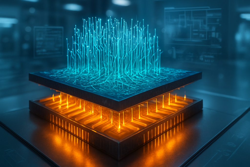
For decades, microchips were built like a house where the plumbing and the electrical wiring were forced to run through the same narrow hallways as the residents. In traditional Front-End-Of-Line (FEOL) manufacturing, both power lines and signal interconnects are built on the front side of the silicon wafer. As transistors shrank to the 3nm level, these wires became so densely packed that they began to interfere with one another, causing significant electrical resistance and "crosstalk" interference.
BSPDN solves this by essentially flipping the house. In this new architecture, the silicon wafer is thinned down to a fraction of its original thickness, and an entirely separate network of power delivery lines is fabricated on the back. Intel Corporation (NASDAQ: INTC) was the first to commercialize this with its PowerVia technology, which utilizes "nano-Through Silicon Vias" (nTSVs) to carry power directly to the transistor layer. This separation allows for much thicker, less resistive power wires on the back and clearer, more efficient signal routing on the front.
The technical specifications are staggering. Early reports from the 1.8nm (18A) production lines indicate that BSPDN reduces "IR drop"—a phenomenon where voltage decreases as it travels through a circuit—by nearly 30%. This allows transistors to switch faster while consuming less energy. Initial reactions from the research community have highlighted that this shift provides a 6% to 10% frequency boost and up to a 15% reduction in total power loss, a critical requirement for AI chips that are now pushing toward 1,000-watt power envelopes.
The New Foundry War: Intel, TSMC, and the 2nm Gold Rush
The successful rollout of BSPDN has reshaped the competitive landscape among the world’s leading foundries. Intel (NASDAQ: INTC) has used its first-mover advantage with PowerVia to reclaim a seat at the table of leading-edge manufacturing. Its 18A node is now in high-volume production, powering the new Panther Lake processors and securing major foundry customers like Microsoft Corporation (NASDAQ: MSFT) and Amazon (NASDAQ: AMZN), both of which are designing custom AI silicon to reduce their reliance on merchant hardware.
However, Taiwan Semiconductor Manufacturing Company (NYSE: TSM) remains the titan to beat. While TSMC’s initial 2nm (N2) node did not include backside power, its upcoming A16 node—scheduled for mass production later this year—introduces the "Super Power Rail." This implementation is even more advanced than Intel's, connecting power directly to the transistor’s source and drain. This precision has led NVIDIA Corporation (NASDAQ: NVDA) to select TSMC’s A16 for its next-generation "Rubin" AI platform, which aims to deliver a 3x performance-per-watt improvement over the previous Blackwell architecture.
Meanwhile, Samsung Electronics (OTC: SSNLF) is positioning itself as the "turnkey" alternative. Samsung is skipping the intermediate steps and moving directly to a highly optimized BSPDN on its 2nm (SF2Z) node. By offering a bundled package of 2nm logic, HBM4 memory, and advanced 2.5D packaging, Samsung has managed to peel away high-profile AI startups and even secure contracts from Advanced Micro Devices (NASDAQ: AMD) for specialized AI chiplets.
AI Scaling and the "Joule-per-Token" Metric
The broader significance of Backside Power Delivery lies in its impact on the economics of artificial intelligence. In 2026, the focus of the AI industry has shifted from raw FLOPS (Floating Point Operations Per Second) to "Joules-per-Token"—a measure of how much energy it takes to generate a single word of AI output. With the cost of 2nm wafers reportedly reaching $30,000 each, the energy efficiency provided by BSPDN is the only way for hyperscalers to keep the operational costs of LLMs (Large Language Models) sustainable.
Furthermore, BSPDN is a prerequisite for the continued density of AI accelerators. By freeing up space on the front of the die, designers have been able to increase logic density by 10% to 20%, allowing for more Tensor cores and larger on-chip caches. This is vital for the 2026 crop of "Superchips" that integrate CPUs and GPUs on a single package. Without backside power, these chips would have simply melted under the thermal and electrical stress of modern AI workloads.
However, this transition has not been without its challenges. One major concern is thermal management. Because the power delivery network is now on the back of the chip, it can trap heat between the silicon and the cooling solution. This has made liquid cooling a mandatory requirement for almost all high-performance AI hardware using these new nodes, leading to a massive infrastructure upgrade cycle in data centers across the globe.
Looking Ahead: 1nm and the 3D Future
The shift to BSPDN is not just a one-time upgrade; it is the foundation for the next decade of semiconductor evolution. Looking forward to 2027 and 2028, experts predict the arrival of the 1.4nm and 1nm nodes, where BSPDN will be combined with "Complementary FET" (CFET) architectures. In a CFET design, n-type and p-type transistors are stacked directly on top of each other, a move that would be physically impossible without the backside plumbing provided by BSPDN.
We are also seeing the early stages of "Function-Side Power Delivery," where specific parts of the chip can be powered independently from the back to allow for ultra-fine-grained power gating. This would allow AI chips to "turn off" 90% of their circuits during idle periods, further driving down the carbon footprint of AI. The primary challenge remaining is yield; as of early 2026, Intel and TSMC are still working to push 2nm/1.8nm yields past the 70% mark, a task complicated by the extreme precision required to align the front and back of the wafer.
A Fundamental Transformation of Silicon
The arrival of Backside Power Delivery marks the end of the "Planar Era" and the beginning of a truly three-dimensional approach to computing. By separating the flow of energy from the flow of information, the semiconductor industry has successfully navigated the most dangerous bottleneck in its history.
The key takeaways for the coming year are clear: Intel has proven its technical relevance with PowerVia, but TSMC’s A16 remains the preferred choice for the highest-end AI hardware. For the tech industry, the 2nm and 1.8nm nodes represent more than just a shrink; they are an architectural rebirth that will define the performance limits of artificial intelligence for years to come. In the coming months, watch for the first third-party benchmarks of Intel’s 18A and the official tape-outs of NVIDIA’s Rubin GPUs—these will be the ultimate tests of whether the "backside revolution" lives up to its immense promise.
This content is intended for informational purposes only and represents analysis of current AI developments.
TokenRing AI delivers enterprise-grade solutions for multi-agent AI workflow orchestration, AI-powered development tools, and seamless remote collaboration platforms.
For more information, visit https://www.tokenring.ai/.