Rabbit Product Design, a product design consulting firm, has updated its electronic design services for IoT devices.
-- Inventors who are interested in developing an IoT product but don’t want to risk expensive manufacturing delays due to unforeseen design flaws can contact Rabbit Product Design to access its recently announced prototyping and manufacturing services. The company manages aspects of the development process, including PCB design and validation.
For more information, please visit https://www.rabbitproductdesign.com/electronicsdesign
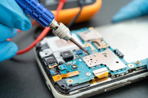
Modern IoT devices, especially wearables, have become smaller to meet consumer demand and, accordingly, require smaller and denser printed circuit boards (PCBs). Experts at Rabbit Product Design say that this kind of miniaturization can create challenges for developers, who must increase circuit complexity while keeping component sizes small; at the same time, the device must use power efficiently, enable wireless connectivity, manage thermal load, and be durable enough to withstand harsh environmental conditions in order to compete with other products on the market.
With so many considerations, extensive simulation and virtual prototyping are necessary to ensure the proposed product functions as intended. For this reason, the team says that IoT inventors should consider working with expert electronics and hardware designers, who often have insights into the latest technologies and trends and employ professional-grade tools for reliable prototyping and validation.
Additionally, professional designers can reduce the time to market by accelerating the development process, resulting in faster launches, often at lower costs.
With a team of senior-level designers with an average of 27 years of experience in the industry, Rabbit Product Design can provide full-service product development for IoT devices. As part of the process, the team first researches the main components required for the client’s product, creates a block diagram, and then uses advanced PCB design software to make a schematic. A prototype PCB is designed based on the schematic, and this design undergoes a review before it is sent for a prototype quote.
Once the review is complete, the components are ordered and soldered to the PCB through wave solder or hole technology. The bare board is inspected before being tested for functionality, allowing the team to identify errors early on in the development process.
Aside from prototyping, Rabbit Product Design can provide factory sourcing, production tooling, packaging, and marketing support as part of its end-to-end services.
Interested parties can learn more by visiting https://www.rabbitproductdesign.com/
Contact Info:
Name: Adam Tavin
Email: Send Email
Organization: Rabbit Product Design
Address: 2100 Geng Rd Ste 210, Palo Alto, CA 94303, United States
Website: https://www.rabbitproductdesign.com/
Source: PressCable
Release ID: 89183499
Should there be any problems, inaccuracies, or doubts arising from the content provided in this press release that require attention or if a press release needs to be taken down, we urge you to notify us immediately by contacting error@releasecontact.com (it is important to note that this email is the authorized channel for such matters, sending multiple emails to multiple addresses does not necessarily help expedite your request). Our efficient team will promptly address your concerns within 8 hours, taking necessary steps to rectify identified issues or assist with the removal process. Providing accurate and dependable information is central to our commitment.