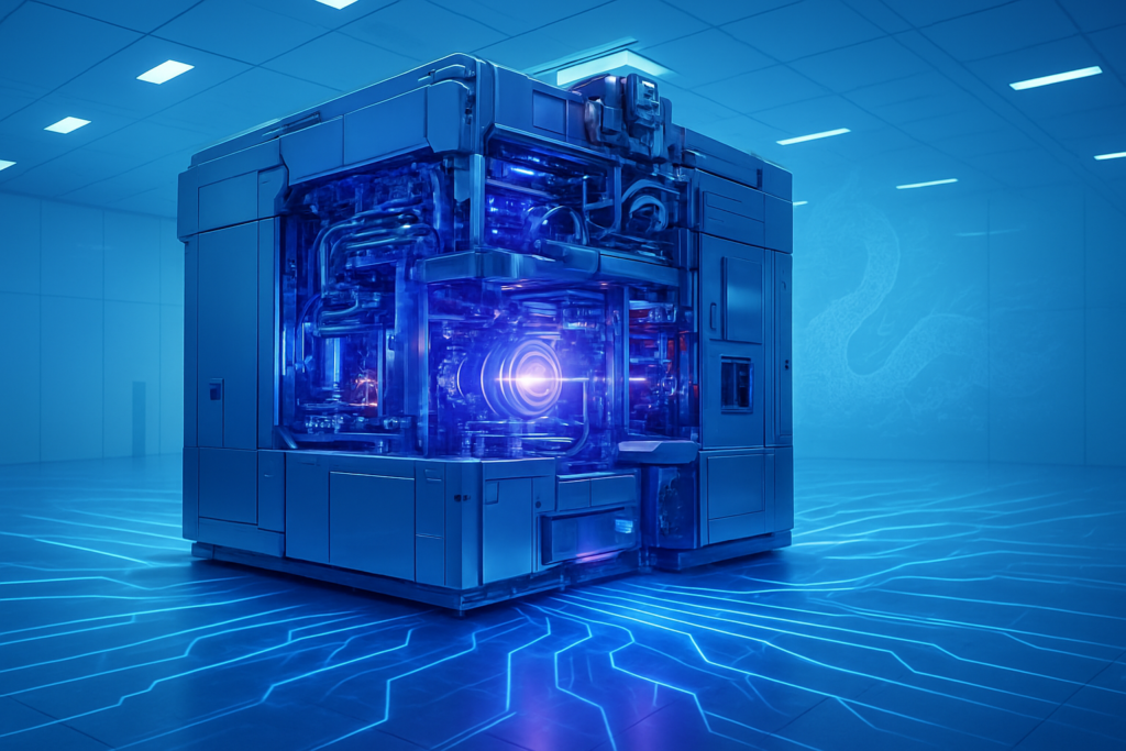
In a development poised to dramatically reshape the global semiconductor industry, China has reportedly completed a prototype Extreme Ultraviolet (EUV) lithography machine, marking a significant leap in its ambitious "Manhattan Project" to achieve chip sovereignty. This technological breakthrough, confirmed by reports in early 2025, signifies a direct challenge to the long-standing monopoly held by Dutch giant ASML Holding N.V. (AMS: ASML) in the advanced chipmaking arena. The immediate significance of this achievement cannot be overstated: it represents a critical step for Beijing in bypassing stringent US-led export controls and securing an independent supply chain for the cutting-edge semiconductors vital for artificial intelligence, 5G, and advanced military applications.
The initiative, characterized by its secrecy, state-driven funding, and a "whole-of-nation" approach, underscores China's unwavering commitment to technological self-reliance. While the prototype has successfully generated EUV light—the essential ingredient for advanced chipmaking—it has yet to produce functional chips. Nevertheless, its existence alone signals China's potential to disrupt the delicate balance of power in the tech world, demonstrating a resolve to overcome external dependencies and establish itself as a formidable player at the forefront of semiconductor innovation.
Technical Prowess and the Road Less Traveled
The completion of China's prototype EUV lithography machine in early 2025, within a highly secure laboratory in Shenzhen, represents a monumental engineering feat. This colossal apparatus, sprawling across nearly an entire factory floor, is currently undergoing rigorous testing. The core achievement lies in its ability to generate extreme ultraviolet light, a fundamental requirement for etching the minuscule patterns on silicon wafers that form advanced chips. While ASML's commercial EUV systems utilize a Laser Produced Plasma (LPP) light source, reports indicate that Chinese electronics giant Huawei Technologies Co., Ltd. (SHE: 002502) is actively testing an alternative Laser Discharge Induced Plasma (LDP) light source at its Dongguan facility, with trial production of circuits reportedly commencing in the third quarter of 2025. This LDP method is even speculated by some experts to potentially offer greater efficiency than ASML's established LPP technology.
The development effort has reportedly been bolstered by a team comprising former engineers from ASML, who are believed to have reverse-engineered critical aspects of the Dutch firm's technology. To circumvent export restrictions, China has resourcefuly sourced parts from older ASML machines available on secondary markets, alongside components from Japanese suppliers like Nikon Corp. (TYO: 7731) and Canon Inc. (TYO: 7751). However, a key challenge remains the acquisition of high-precision optical systems, traditionally supplied by specialized firms like Germany's Carl Zeiss AG, a crucial ASML partner. This reliance on alternative sourcing and reverse engineering has resulted in a prototype that is reportedly significantly larger and less refined than ASML's commercial offerings.
Despite these hurdles, the functionality of the Chinese prototype in generating EUV light marks a critical divergence from previous approaches, which primarily relied on Deep Ultraviolet (DUV) lithography combined with complex multi-patterning techniques to achieve smaller nodes—a method fraught with yield challenges. While ASML CEO Christophe Fouquet stated in April 2025 that China would need "many, many years" to develop such technology, the swift emergence of this prototype suggests a significantly accelerated timeline. China's ambitious target is to produce working chips from its domestic EUV machine by 2028, with 2030 being considered a more realistic timeframe by many industry observers. This indigenous development promises to free Chinese chipmakers from the technological stagnation imposed by international sanctions, offering a pathway to genuinely compete at the leading edge of semiconductor manufacturing.
Shifting Tides: Competitive Implications for Global Tech Giants
China's accelerated progress in domestic EUV lithography, spearheaded by Huawei Technologies Co., Ltd. (SHE: 002502) and Semiconductor Manufacturing International Corporation (SMIC) (HKG: 0981), is poised to trigger a significant reordering of the global technology landscape. The most immediate beneficiaries are Chinese semiconductor manufacturers and tech giants. SMIC, for instance, is reportedly on track to finalize its 5nm chip development by the end of 2025, with Huawei planning to leverage this advanced process for its Ascend 910C AI chip. Huawei itself is aggressively scaling its Ascend AI chip production, aiming to double output in 2025 to approximately 600,000 units, with plans to further increase total output to as many as 1.6 million dies in 2026. This domestic capability will provide a reliable, sanction-proof source of high-performance chips for Chinese tech companies like Alibaba Group Holding Ltd. (NYSE: BABA), DeepSeek, Tencent Holdings Ltd. (HKG: 0700), and Baidu, Inc. (NASDAQ: BIDU), ensuring the continuity and expansion of their AI operations and cloud services within China. Furthermore, the availability of advanced domestic chips is expected to foster a more vibrant ecosystem for Chinese AI startups, potentially lowering entry barriers and accelerating indigenous innovation.
The competitive implications for Western chipmakers are profound. Companies like NVIDIA Corporation (NASDAQ: NVDA), Advanced Micro Devices, Inc. (NASDAQ: AMD), and Intel Corporation (NASDAQ: INTC), which have historically dominated the high-performance chip market, face a long-term threat to their market share within China and potentially beyond. While NVIDIA's newest Grace Blackwell series processors are seeing strong global demand, its dominance in China is demonstrably weakening due to export controls and the rapid ascent of Huawei's Ascend processors. Reports from early 2025 even suggested that some Chinese-designed AI accelerators were processing complex algorithms more efficiently than certain NVIDIA offerings. If China successfully scales its domestic EUV production, it could bypass Western restrictions on cutting-edge nodes (e.g., 5nm, 3nm), directly impacting the revenue streams of these global leaders.
Global foundries like Taiwan Semiconductor Manufacturing Company Limited (TSMC) (NYSE: TSM) and Samsung Electronics Co., Ltd. (KRX: 005930), currently at the forefront of advanced chip manufacturing with ASML's EUV machines, could also face increased competition from SMIC. While SMIC's 5nm wafer costs are presently estimated to be up to 50% higher than TSMC's, coupled with lower yields due to its reliance on DUV for these nodes, successful domestic EUV implementation could significantly narrow this gap. For ASML Holding N.V. (AMS: ASML), the current undisputed monarch of EUV technology, China's commercialization of LDP-based EUV would directly challenge its monopoly. ASML CEO Christophe Fouquet has acknowledged that "China will not accept to be cut off from technology," highlighting the inevitability of China's pursuit of self-sufficiency. This intense competition is likely to accelerate efforts among global tech companies to diversify supply chains, potentially leading to a "decoupling" of technological ecosystems and the emergence of distinct standards and suppliers in China.
Strategically, China's domestic EUV breakthrough grants it unparalleled technological autonomy and national security in advanced semiconductor manufacturing, aligning with the core objectives of its "Made in China 2025" initiative. Huawei, at the helm of this national strategy, is actively building a parallel, independent ecosystem for AI infrastructure, demonstrating a commitment to compensating for limited Western EUV access through alternative architectural strategies and massive domestic production scaling. This geopolitical rebalancing underscores that strategic pressure and export controls can, paradoxically, accelerate indigenous innovation. The success of China's EUV project will likely force a re-evaluation of current export control policies by the US and its allies, as the world grapples with the implications of a truly self-reliant Chinese semiconductor industry.
A New Epoch: Broader Implications for the AI Landscape and Geopolitics
The emergence of China's prototype EUV lithography machine in late 2025 is more than just a technical achievement; it is a foundational hardware breakthrough that will profoundly influence the broader Artificial Intelligence landscape and global geopolitical dynamics. EUV lithography is the linchpin for manufacturing the high-performance, energy-efficient chips with sub-7nm, 5nm, 3nm, and even sub-2nm nodes that are indispensable for powering modern AI applications—from sophisticated AI accelerators and neural processing units to large language models and advanced AI hardware for data centers, autonomous systems, and military technologies. Without such advanced manufacturing capabilities, the rapid advancements observed in AI development would face insurmountable obstacles. China's domestic EUV effort is thus a cornerstone of its strategy to achieve self-sufficiency in AI, mitigate the impact of U.S. export controls, and accelerate its indigenous AI research and deployment, effectively securing the "compute" power that has become the defining constraint for AI progress.
The successful development and eventual mass production of China's EUV lithography machine carries multifaceted impacts. Geopolitically and economically, it promises to significantly reduce China's dependence on foreign technology, particularly ASML Holding N.V.'s (AMS: ASML) EUV systems, thereby enhancing its national security and resilience against export restrictions. This breakthrough could fundamentally alter the global technological balance, intensifying the ongoing "tech cold war" and challenging the West's historical monopoly on cutting-edge chipmaking technology. While it poses a potential threat to ASML's market dominance, it could also introduce new competition in the high-end lithography market, leading to shifts in global supply chains. However, the dual-use potential of advanced AI chips—serving both commercial and military applications—raises significant concerns and could further fuel geopolitical tensions regarding military-technological parity. Technologically, domestic access to EUV would enable China to produce its own cutting-edge AI chips, accelerating its progress in AI research, hardware development, and deployment across various sectors, facilitating new AI hardware architectures crucial for optimizing AI workloads, and potentially narrowing the node gap with leading manufacturers to 5nm, 3nm, or even 2nm by 2030.
Despite the strategic advantages for China, this development also brings forth several concerns. The technical viability and quality of scaling production, ensuring sustained reliability, achieving comparable throughput, and replicating the precision optical systems of ASML's machines remain significant hurdles. Moreover, the reported reverse-engineering of ASML technology raises intellectual property infringement concerns. Geopolitical escalation is another real risk, as China's success could provoke further export controls and trade restrictions from the U.S. and its allies. The energy consumption of EUV lithography, an incredibly power-intensive process, also poses sustainability challenges as China ramps up its chip production. Furthermore, a faster, unrestrained acceleration of AI development in China, potentially without robust international ethical frameworks, could lead to novel ethical dilemmas and risks on a global scale.
In the broader context of AI milestones, China's prototype EUV machine can be seen as a foundational hardware breakthrough, akin to previous pivotal moments. Just as powerful GPUs from companies like NVIDIA Corporation (NASDAQ: NVDA) provided the computational backbone for the deep learning revolution, EUV lithography acts as the "unseen engine" that enables the complex designs and high transistor densities required for sophisticated AI algorithms. This intense global investment in advanced chip manufacturing and AI infrastructure mirrors the scale of the dot-com boom or the expansion of cloud computing infrastructure. The fierce competition over AI chips and underlying manufacturing technology like EUV reflects a modern-day scramble for vital strategic resources. The U.S.-China AI rivalry, driven by the race for technological supremacy, is frequently compared to the nuclear arms race of the Cold War era. China's rapid progress in EUV lithography, spurred by export controls, exemplifies how strategic pressure can accelerate domestic innovation in critical technologies, a "DeepSeek moment for lithography" that parallels how Chinese AI models have rapidly caught up to and even rivaled leading Western models despite chip restrictions. This monumental effort underscores a profound shift in the global semiconductor and AI landscapes, intensifying geopolitical competition and potentially reshaping supply chains for decades to come.
The Road Ahead: China's Ambitions and the Future of Advanced Chipmaking
The journey from a prototype EUV lithography machine to commercially viable, mass-produced advanced chips is fraught with challenges, yet China's trajectory indicates a determined march towards its goals. In the near term, the focus is squarely on transitioning from successful EUV light generation to the production of functional chips. With a prototype already undergoing testing at facilities like Huawei Technologies Co., Ltd.'s (SHE: 002502) Dongguan plant, the critical next steps involve optimizing the entire manufacturing process. Trial production of circuits using these domestic systems reportedly commenced in the second or third quarter of 2025, with ambitious plans for full-scale or mass production slated for 2026. This period will be crucial for refining the Laser-Induced Discharge Plasma (LDP) method, which Chinese institutions like the Harbin Institute of Technology and the Shanghai Institute of Optics and Fine Mechanics are championing as an alternative to ASML Holding N.V.'s (AMS: ASML) Laser-Produced Plasma (LPP) technology. Success in this phase would validate the LDP approach and potentially offer a simpler, more cost-effective, and energy-efficient pathway to EUV.
Looking further ahead, China aims to produce functional chips from its EUV prototypes by 2028, with 2030 being a more realistic target for achieving significant commercial output. The long-term vision is nothing less than complete self-sufficiency in advanced chip manufacturing. Should China successfully commercialize LDP-based EUV lithography, it would become the only nation outside the Netherlands with such advanced capabilities, fundamentally disrupting the global semiconductor industry. Experts predict that if China can advance to 3nm or even 2nm chip production by 2030, it could emerge as a formidable competitor to established leaders like ASML, Taiwan Semiconductor Manufacturing Company Limited (TSMC) (NYSE: TSM), and Samsung Electronics Co., Ltd. (KRX: 005930). This would unlock the domestic manufacturing of chips smaller than 7 nanometers, crucial for powering advanced Artificial Intelligence (AI) systems, military applications, next-generation smartphones, and high-performance computing, thereby significantly strengthening China's position in these strategic sectors.
However, the path to commercial viability is riddled with formidable challenges. Technical optimization remains paramount, particularly in boosting the power output of LDP systems, which currently range from 50-100W but require at least 250W for commercial scale. Replicating the extreme precision of Western optical systems, especially those from Carl Zeiss AG, and developing a comprehensive domestic ecosystem for all critical components—including pellicles, masks, and resist materials—are significant bottlenecks. System integration, given the immense complexity of an EUV scanner, also presents considerable engineering hurdles. Beyond the technical, geopolitical and supply chain restrictions continue to loom, with the risk of further export controls on essential materials and components. While China has leveraged parts from older ASML machines obtained from secondary markets, this approach may not be sustainable or scalable for cutting-edge nodes.
Expert predictions, while acknowledging China's remarkable progress, largely agree that scaling EUV production to commercially competitive levels will take considerable time. While some researchers, including those from TSMC, have optimistically suggested that China's LDP method could "out-compete ASML," most analysts believe that initial production capacity will likely be constrained. The unwavering commitment of the Chinese government, often likened to a "Manhattan Project," coupled with substantial investments and coordinated efforts across various research institutes and companies like Huawei, is a powerful driving force. This integrated approach, encompassing chip design to fabrication equipment, aims to entirely bypass foreign tech restrictions. The rate of China's progress towards self-sufficiency in advanced semiconductors will ultimately be determined by its ability to overcome these technological complexities and market dynamics, rather than solely by the impact of export controls, fundamentally reshaping the global semiconductor landscape in the coming years.
The Dawn of a New Era: A Comprehensive Wrap-up
China's "Manhattan Project" to develop a domestic EUV lithography machine has culminated in the successful creation of a working prototype, a monumental achievement that, as of December 2025, signals a pivotal moment in the global technology race. This breakthrough, driven by an unwavering national imperative for chip sovereignty, represents a direct response to stringent U.S.-led export controls and a strategic move to secure an independent supply chain for advanced semiconductors. Key takeaways include the prototype's ability to generate extreme ultraviolet light, its reliance on a combination of reverse engineering from older ASML Holding N.V. (AMS: ASML) machines, and the innovative adoption of Laser-Induced Discharge Plasma (LDP) technology, which some experts believe could offer advantages over ASML's LPP method. Huawei Technologies Co., Ltd. (SHE: 002502) stands at the forefront of this coordinated national effort, aiming to establish an entire domestic AI supply chain. While the prototype has yet to produce functional chips, with targets set for 2028 and a more realistic outlook of 2030, the progress is undeniable.
This development holds immense significance in the history of Artificial Intelligence. Advanced AI systems, particularly those underpinning large language models and complex neural networks, demand cutting-edge chips with unparalleled processing power and efficiency—chips predominantly manufactured using EUV lithography. China's ability to master this technology and produce advanced chips domestically would dramatically reduce its strategic dependence on foreign suppliers for the foundational hardware of AI. This would not only enable China to accelerate its AI development independently, free from external bottlenecks, but also potentially shift the global balance of power in AI research and application, bolstering Beijing's quest for leadership in AI and military-technological parity.
The long-term impact of China's EUV lithography project is poised to be profound and transformative. Should China successfully transition from a functional prototype to commercial-scale production of advanced chips by 2030, it would fundamentally redefine global semiconductor supply chains, challenging ASML's near-monopoly and ushering in a more multipolar semiconductor industry. This achievement would represent a major victory in China's "Made in China 2025" and subsequent self-reliance initiatives, significantly reducing its vulnerability to foreign export controls. While accelerating China's AI development, such a breakthrough is also likely to intensify geopolitical tensions, potentially prompting further countermeasures and heightened competition in the tech sphere.
In the coming weeks and months, the world will be closely watching for several critical indicators. The most immediate milestone is the prototype's transition from generating EUV light to successfully producing working semiconductor chips, with performance metrics such as resolution capabilities, throughput stability, and yield rates being crucial. Further advancements in LDP technology, particularly in efficiency and power output, will demonstrate China's capacity for innovation beyond reverse-engineering. The specifics of China's 15th five-year plan (2026-2030), expected to be fully detailed next year, will reveal the continued scale of investment and strategic focus on semiconductor and AI self-reliance. Finally, any new export controls or diplomatic discussions from the U.S. and its allies in response to China's demonstrated progress will be closely scrutinized, as the global tech landscape continues to navigate this new era of intensified competition and technological independence.
This content is intended for informational purposes only and represents analysis of current AI developments.
TokenRing AI delivers enterprise-grade solutions for multi-agent AI workflow orchestration, AI-powered development tools, and seamless remote collaboration platforms.
For more information, visit https://www.tokenring.ai/.