The semiconductor industry is abuzz with speculation surrounding Taiwan Semiconductor Manufacturing Company's (TSMC) (NYSE: TSM) highly anticipated 2nm (N2) process node. Whispers from within the supply chain suggest that while N2 represents a significant leap forward in manufacturing technology, its power, performance, and area (PPA) improvements might be more incremental than the dramatic generational gains seen in the past. This nuanced advancement has profound implications, particularly for major clients like Apple (NASDAQ: AAPL) and the burgeoning field of next-generation AI chip development, where every nanometer and every watt counts.
As the industry grapples with the escalating costs of advanced silicon, the perceived moderation in N2's PPA gains could reshape strategic decisions for tech giants. While some reports suggest this might lead to less astronomical cost increases per wafer, others indicate N2 wafers will still be significantly pricier. Regardless, the transition to N2, slated for mass production in the second half of 2025 with strong demand already reported for 2026, marks a pivotal moment, introducing Gate-All-Around (GAAFET) transistors and intensifying the race among leading foundries like Samsung and Intel to dominate the sub-3nm era. The efficiency gains, even if incremental, are critical for AI data centers facing unprecedented power consumption challenges.
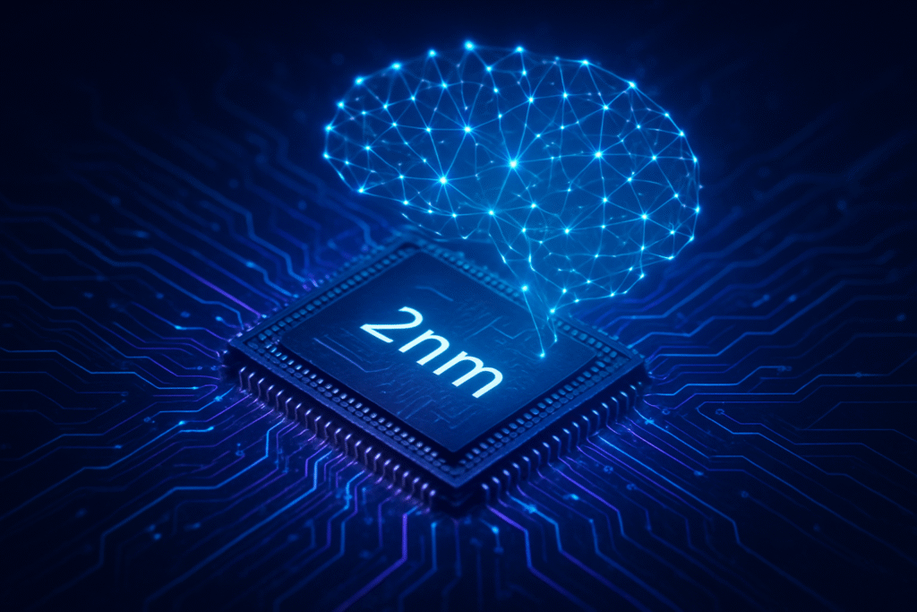
The Architectural Leap: GAAFETs and Nuanced PPA Gains Define TSMC's N2
TSMC's 2nm (N2) process node, slated for mass production in the second half of 2025 following risk production commencement in July 2024, represents a monumental architectural shift for the foundry. For the first time, TSMC is moving away from the long-standing FinFET (Fin Field-Effect Transistor) architecture, which has dominated advanced nodes for over a decade, to embrace Gate-All-Around (GAAFET) nanosheet transistors. This transition is not merely an evolutionary step but a fundamental re-engineering of the transistor structure, crucial for continued scaling and performance enhancements in the sub-3nm era.
In FinFETs, the gate controls the current flow by wrapping around three sides of a vertical silicon fin. While a significant improvement over planar transistors, GAAFETs offer superior electrostatic control by completely encircling horizontally stacked silicon nanosheets that form the transistor channel. This full encirclement leads to several critical advantages: significantly reduced leakage current, improved current drive, and the ability to operate at lower voltages, all contributing to enhanced power efficiency—a paramount concern for modern high-performance computing (HPC) and AI workloads. Furthermore, GAA nanosheets offer design flexibility, allowing engineers to adjust channel widths to optimize for specific performance or power targets, a feature TSMC terms NanoFlex.
Despite some initial rumors suggesting limited PPA improvements, TSMC's official projections indicate robust gains over its 3nm N3E node. N2 is expected to deliver a 10% to 15% speed improvement at the same power consumption, or a 25% to 30% reduction in power consumption at the same speed. The transistor density is projected to increase by 15% (1.15x) compared to N3E. Subsequent iterations like N2P promise even further enhancements, with an 18% speed improvement and a 36% power reduction. These gains are further bolstered by innovations like barrier-free tungsten wiring, which reduces resistance by 20% in the middle-of-line (MoL).
The AI research community and industry experts have reacted with "unprecedented" demand for N2, particularly from the HPC and AI sectors. Over 15 major customers, with about 10 focused on AI applications, have committed to N2. This signals a clear shift where AI's insatiable computational needs are now the primary driver for cutting-edge chip technology, surpassing even smartphones. Companies like NVIDIA (NASDAQ: NVDA), AMD (NASDAQ: AMD), Apple (NASDAQ: AAPL), Qualcomm (NASDAQ: QCOM), and others are heavily invested, recognizing that N2's significant power reduction capabilities (30-40%) are vital for mitigating the escalating electricity demands of AI data centers. Initial defect density and SRAM yield rates for N2 are reportedly strong, indicating a smooth path towards volume production and reinforcing industry confidence in this pivotal node.
The AI Imperative: N2's Influence on Next-Gen Processors and Competitive Dynamics
The technical specifications and cost implications of TSMC's N2 process are poised to profoundly influence the product roadmaps and competitive strategies of major AI chip developers, including Apple (NASDAQ: AAPL) and Qualcomm (NASDAQ: QCOM). While the N2 node promises substantial PPA improvements—a 10-15% speed increase or 25-30% power reduction, alongside a 15% transistor density boost over N3E—these advancements come at a significant price, with N2 wafers projected to cost between $30,000 and $33,000, a potential 66% hike over N3 wafers. This financial reality is shaping how companies approach their next-generation AI silicon.
For Apple, a perennial alpha customer for TSMC's most advanced nodes, N2 is critical for extending its leadership in on-device AI. The A20 chip, anticipated for the iPhone 18 series in 2026, and future M-series processors (like the M5) for Macs, are expected to leverage N2. These chips will power increasingly sophisticated on-device AI capabilities, from enhanced computational photography to advanced natural language processing. Apple has reportedly secured nearly half of the initial N2 production, ensuring its premium devices maintain a cutting edge. However, the high wafer costs might lead to a tiered adoption, with only Pro models initially featuring the 2nm silicon, impacting the broader market penetration of this advanced technology. Apple's deep integration with TSMC, including collaboration on future 1.4nm nodes, underscores its commitment to maintaining a leading position in silicon innovation.
Qualcomm (NASDAQ: QCOM), a dominant force in the Android ecosystem, is taking a more diversified and aggressive approach. Rumors suggest Qualcomm intends to bypass the standard N2 node and move directly to TSMC's more advanced N2P process for its Snapdragon 8 Elite Gen 6 and Gen 7 chipsets, expected in 2026. This strategy aims to "squeeze every last bit of performance" for its on-device Generative AI capabilities, crucial for maintaining competitiveness against rivals. Simultaneously, Qualcomm is actively validating Samsung Foundry's (KRX: 005930) 2nm process (SF2) for its upcoming Snapdragon 8 Elite 2 chip. This dual-sourcing strategy mitigates reliance on a single foundry, enhances supply chain resilience, and provides leverage in negotiations, a prudent move given the increasing geopolitical and economic complexities of semiconductor manufacturing.
Beyond these mobile giants, the impact of N2 reverberates across the entire AI landscape. High-Performance Computing (HPC) and AI sectors are the primary drivers of N2 demand, with approximately 10 of the 15 major N2 clients being HPC-oriented. Companies like NVIDIA (NASDAQ: NVDA) for its Rubin Ultra GPUs and AMD (NASDAQ: AMD) for its Instinct MI450 accelerators are poised to leverage N2 for their next-generation AI chips, demanding unparalleled computational power and efficiency. Hyperscalers such as Google (NASDAQ: GOOGL), Amazon (NASDAQ: AMZN), and OpenAI are also designing custom AI ASICs that will undoubtedly benefit from the PPA advantages of N2. The intense competition also highlights the efforts of Intel Foundry (NASDAQ: INTC), whose 18A (1.8nm-class) process, featuring RibbonFET (GAA) and PowerVia (backside power delivery), is positioned as a strong contender, aiming for mass production by late 2025 or early 2026 and potentially offering unique advantages that TSMC won't implement until its A16 node.
Beyond the Nanometer: N2's Broader Impact on AI Supremacy and Global Dynamics
TSMC's 2nm (N2) process technology, with its groundbreaking transition to Gate-All-Around (GAAFET) transistors and significant PPA improvements, extends far beyond mere chip specifications; it profoundly influences the global race for AI supremacy and the broader semiconductor industry's strategic landscape. The N2 node, set for mass production in late 2025, is poised to be a critical enabler for the next generation of AI, particularly for increasingly complex models like large language models (LLMs) and generative AI, demanding unprecedented computational power.
The PPA gains offered by N2—a 10-15% performance boost at constant power or 25-30% power reduction at constant speed compared to N3E, alongside a 15% increase in transistor density—are vital for extending Moore's Law and fueling AI innovation. The adoption of GAAFETs, a fundamental architectural shift from FinFETs, provides the fundamental control necessary for transistors at this scale, and the subsequent iterations like N2P and A16, incorporating backside power delivery, will further optimize these gains. For AI, where every watt saved and every transistor added contributes directly to the speed and efficiency of training and inference, N2 is not just an upgrade; it's a necessity.
However, this advancement comes with significant concerns. The cost of N2 wafers is projected to be TSMC's most expensive yet, potentially exceeding $30,000 per wafer—a substantial increase that will inevitably be passed on to consumers. This exponential rise in manufacturing costs, driven by immense R&D and capital expenditure for GAAFET technology and extensive Extreme Ultraviolet (EUV) lithography steps, poses a challenge for market accessibility and could lead to higher prices for next-generation products. The complexity of the N2 process also introduces new manufacturing hurdles, requiring sophisticated design and production techniques.
Furthermore, the concentration of advanced manufacturing capabilities, predominantly in Taiwan, raises critical supply chain concerns. Geopolitical tensions pose a tangible threat to the global semiconductor supply, underscoring the strategic importance of advanced chip production for national security and economic stability. While TSMC is expanding its global footprint with new fabs in Arizona and Japan, Taiwan remains the epicenter of its most advanced operations, highlighting the need for continued diversification and resilience in the global semiconductor ecosystem.
Crucially, N2 addresses one of the most pressing challenges facing the AI industry: energy consumption. AI data centers are becoming enormous power hogs, with global electricity use projected to more double by 2030, largely driven by AI workloads. The 25-30% power reduction offered by N2 chips is essential for mitigating this escalating energy demand, allowing for more powerful AI compute within existing power envelopes and reducing the carbon footprint of data centers. This focus on efficiency, coupled with advancements in packaging technologies like System-on-Wafer-X (SoW-X) that integrate multiple chips and optical interconnects, is vital for overcoming the "fundamental physical problem" of moving data and managing heat in the era of increasingly powerful AI.
The Road Ahead: N2 Variants, 1.4nm, and the AI-Driven Semiconductor Horizon
The introduction of TSMC's 2nm (N2) process node in the second half of 2025 marks not an endpoint, but a new beginning in the relentless pursuit of semiconductor advancement. This foundational GAAFET-based node is merely the first step in a meticulously planned roadmap that includes several crucial variants and successor technologies, all geared towards sustaining the explosive growth of AI and high-performance computing.
In the near term, TSMC is poised to introduce N2P in the second half of 2026, which will integrate backside power delivery. This innovative approach separates the power delivery network from the signal network, addressing resistance challenges and promising further improvements in transistor performance and power consumption. Following closely will be the A16 process, also expected in the latter half of 2026, featuring a Superpower Rail Delivery (SPR) nanosheet for backside power delivery. A16 is projected to offer an 8-10% performance boost and a 15-20% improvement in energy efficiency over N2 nodes, showcasing the rapid iteration inherent in advanced manufacturing.
Looking further out, TSMC's roadmap extends to N2X, a high-performance variant tailored for High-Performance Computing (HPC) applications, anticipated for mass production in 2027. N2X will prioritize maximum clock speeds and voltage tolerance, making it ideal for the most demanding AI accelerators and server processors. Beyond 2nm, the industry is already looking towards 1.4nm production around 2027, with future nodes exploring even more radical technologies such as 2D materials, Complementary FETs (CFETs) that vertically stack transistors for ultimate density, and other novel GAA devices. Deep integration with advanced packaging techniques, such as chiplet designs, will become increasingly critical to continue scaling and enhancing system-level performance.
These advanced nodes will unlock a new generation of applications. Flagship mobile SoCs from Apple (NASDAQ: AAPL), Qualcomm (NASDAQ: QCOM), and MediaTek (TPE: 2454) will leverage N2 for extended battery life and enhanced on-device AI capabilities. CPUs and GPUs from AMD (NASDAQ: AMD), NVIDIA (NASDAQ: NVDA), and Intel (NASDAQ: INTC) will utilize N2 for unprecedented AI acceleration in data centers and cloud computing, powering everything from large language models to complex scientific simulations. The automotive industry, with its growing reliance on advanced semiconductors for autonomous driving and ADAS, will also be a significant beneficiary.
However, the path forward is not without its challenges. The escalating cost of manufacturing remains a primary concern, with N2 wafers projected to exceed $30,000. This immense financial burden will continue to drive up the cost of high-end electronics. Achieving consistently high yields with novel architectures like GAAFETs is also paramount for cost-effective mass production. Furthermore, the relentless demand for power efficiency will necessitate continuous innovation, with backside power delivery in N2P and A16 directly addressing this by optimizing power delivery.
Experts universally predict that AI will be the primary catalyst for explosive growth in the semiconductor industry. The AI chip market alone is projected to reach an estimated $323 billion by 2030, with the entire semiconductor industry approaching $1.3 trillion. TSMC is expected to solidify its lead in high-volume GAAFET manufacturing, setting new standards for power efficiency, particularly in mobile and AI compute. Its dominance in advanced nodes, coupled with investments in advanced packaging solutions like CoWoS, will be crucial. While competition from Intel's 18A and Samsung's SF2 will remain fierce, TSMC's strategic positioning and technological prowess are set to define the next era of AI-driven silicon innovation.
Comprehensive Wrap-up: TSMC's N2 — A Defining Moment for AI's Future
The rumors surrounding TSMC's 2nm (N2) process, particularly the initial whispers of limited PPA improvements and the confirmed substantial cost increases, have catalyzed a critical re-evaluation within the semiconductor industry. What emerges is a nuanced picture: N2, with its pivotal transition to Gate-All-Around (GAAFET) transistors, undeniably represents a significant technological leap, offering tangible gains in power efficiency, performance, and transistor density. These improvements, even if deemed "incremental" compared to some past generational shifts, are absolutely essential for sustaining the exponential demands of modern artificial intelligence.
The key takeaway is that N2 is less about a single, dramatic PPA breakthrough and more about a strategic architectural shift that enables continued scaling in the face of physical limitations. The move to GAAFETs provides the fundamental control necessary for transistors at this scale, and the subsequent iterations like N2P and A16, incorporating backside power delivery, will further optimize these gains. For AI, where every watt saved and every transistor added contributes directly to the speed and efficiency of training and inference, N2 is not just an upgrade; it's a necessity.
This development underscores the growing dominance of AI and HPC as the primary drivers of advanced semiconductor manufacturing. Companies like Apple (NASDAQ: AAPL), Qualcomm (NASDAQ: QCOM), NVIDIA (NASDAQ: NVDA), and AMD (NASDAQ: AMD) are making strategic decisions—from early capacity reservations to diversified foundry approaches—to leverage N2's capabilities for their next-generation AI chips. The escalating costs, however, present a formidable challenge, potentially impacting product pricing and market accessibility.
As the industry moves towards 1.4nm and beyond, the focus will intensify on overcoming these cost and complexity hurdles, while simultaneously addressing the critical issue of energy consumption in AI data centers. TSMC's N2 is a defining milestone, marking the point where architectural innovation and power efficiency become paramount. Its significance in AI history will be measured not just by its raw performance, but by its ability to enable the next wave of intelligent systems while navigating the complex economic and geopolitical landscape of global chip manufacturing.
In the coming weeks and months, industry watchers will be keenly observing the N2 production ramp, initial yield rates, and the unveiling of specific products from key customers. The competitive dynamics between TSMC, Samsung, and Intel in the sub-2nm race will intensify, shaping the strategic alliances and supply chain resilience for years to come. The future of AI, inextricably linked to these nanometer-scale advancements, hinges on the successful and widespread adoption of technologies like TSMC's N2.
This content is intended for informational purposes only and represents analysis of current AI developments.
TokenRing AI delivers enterprise-grade solutions for multi-agent AI workflow orchestration, AI-powered development tools, and seamless remote collaboration platforms.
For more information, visit https://www.tokenring.ai/.