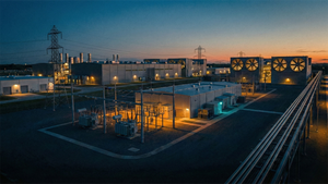
As the artificial intelligence revolution enters its most capital-intensive phase, the industry's focus has shifted from the raw processing power of GPUs to the critical bottleneck of data movement. High Bandwidth Memory (HBM) has emerged as the "fuel" of the AI era, transforming from a niche specialized component into the single most influential driver of the semiconductor supply chain. By late 2025, the demand for these dense, vertically stacked memory chips has reached a fever pitch, creating a massive windfall for the equipment manufacturers that provide the precision tools necessary to build them.
Leading this charge is Lam Research (NASDAQ: LRCX), which has seen its valuation and order books swell as chipmakers race to solve the "memory wall." The current transition from HBM3E to the next-generation HBM4 standard represents more than just a capacity upgrade; it is a fundamental shift in how memory and logic are integrated. As AI models grow to trillions of parameters, the ability to feed data to processors like NVIDIA (NASDAQ: NVDA) Blackwell and Rubin chips has become the primary differentiator in the race for AI supremacy, making the equipment used to etch and plate these chips more valuable than ever.
The Architecture War: From HBM3E to HBM4
The technical landscape of AI memory in late 2025 is defined by the transition from the "capacity war" of HBM3E to the "architecture war" of HBM4. While 12-layer HBM3E remains the current workhorse for data center deployments, the industry has begun the shift toward 16-layer HBM4, which was standardized by JEDEC earlier this year. HBM4 is a landmark development because it doubles the interface width to 2048-bit, allowing for bandwidths exceeding 1.5 TB/s per stack. This leap is necessitated by the massive data throughput requirements of next-generation AI training clusters, which are increasingly limited by the energy and time required to move data between the processor and memory.
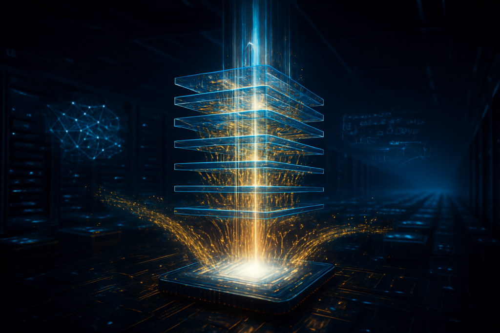
To achieve these specifications, manufacturers are relying on advanced Through-Silicon Via (TSV) technology, where thousands of microscopic holes are drilled through silicon layers to create vertical electrical connections. Lam Research has solidified its position as the gatekeeper of this process with its new Akara etching system. Unlike previous generations, HBM4 requires deeper, narrower vias with virtually zero "scalloping" or roughness on the interior walls. Lam’s Syndion and Akara tools provide the high-aspect-ratio etching needed to stack 16 or even 20 layers of DRAM while maintaining electrical integrity. This is complemented by the SABRE 3D® deposition system, which handles the copper electrofilling of these vias, ensuring void-free connections that are essential for high-yield production.
Initial reactions from the AI research community have been overwhelmingly positive, though tempered by the sheer complexity of the manufacturing process. Experts note that HBM4 marks the first time the "base die"—the bottom layer of the memory stack—is being manufactured on advanced logic nodes (such as 5nm or 12nm) rather than traditional memory processes. This allows the memory stack to handle more complex logic functions, such as error correction and power management, directly on the chip. However, this integration has introduced significant thermal challenges, as stacking logic and memory together creates "hot spots" that can lead to performance throttling if not managed by advanced packaging techniques.
Market Dynamics and the Rise of the Equipment Giants
The financial implications of this memory boom are most visible in the balance sheets of wafer fabrication equipment (WFE) providers. In its October 2025 earnings report, Lam Research posted record Q3 revenue of $5.32 billion, a nearly 28% increase year-over-year. Management highlighted that HBM-related revenue grew by 50% during the same period, far outstripping the growth of the broader semiconductor market. For every dollar invested in AI data centers, a growing percentage is now flowing directly into the specialized etching and deposition tools required for 3D stacking. This has placed Lam Research, along with competitors like Applied Materials (NASDAQ: AMAT) and Tokyo Electron (TYO: 8035), at the center of the AI investment thesis.
In the competitive landscape of memory producers, SK Hynix (KRX: 000660) continues to hold the lion's share of the HBM market, estimated at over 60% as of late 2025. Their "trilateral alliance" with NVIDIA and TSMC (NYSE: TSM) has become the gold standard for AI hardware, utilizing TSMC’s logic process for the HBM4 base die. Meanwhile, Micron (NASDAQ: MU) has successfully climbed to the number two spot, capturing roughly 22% of the market by aggressively scaling its HBM3E production. Samsung (KRX: 005930), while trailing in market share at 16%, is betting heavily on its "all-in-one" capability—acting as the memory maker, foundry, and packager—to regain ground as HBM4 moves into mass production in 2026.
This shift is disrupting the traditional "commodity" nature of the memory market. HBM is no longer a generic part bought in bulk; it is a highly customized, co-designed component that requires deep collaboration between the memory maker and the logic designer (like NVIDIA or AMD). This strategic advantage favors companies that can master the complex packaging and integration steps, effectively raising the barrier to entry and securing long-term supply agreements that were previously unheard of in the volatile DRAM industry.
The Wider Significance: Breaking the Memory Wall
The HBM boom represents a pivotal moment in the history of computing, signaling a move from "compute-centric" to "data-centric" architecture. For decades, processor speeds increased much faster than memory bandwidth, leading to the "memory wall" where CPUs and GPUs spent most of their time waiting for data. By bringing memory physically closer to the logic and stacking it vertically, the industry is effectively trying to collapse the distance data must travel. This is not just about speed; it is about power efficiency. In 2025, data movement accounts for a significant portion of the energy consumed by AI models, and HBM4’s wider interface allows for lower clock speeds at higher bandwidths, significantly reducing the energy-per-bit transferred.
However, this advancement comes with concerns regarding supply chain concentration and cost. The extreme precision required by Lam Research's tools and the low yields associated with 16-layer stacking have kept HBM prices high. This has led to a "compute divide," where only the largest tech giants—the so-called "Hyperscalers"—can afford the massive HBM-laden clusters required to train the next generation of frontier models. Critics argue that this concentration of hardware power could stifle innovation among smaller startups and academic institutions that cannot compete with the capital expenditures of companies like Microsoft (NASDAQ: MSFT) or Meta (NASDAQ: META).
Furthermore, the integration of memory and logic via HBM4 is a precursor to "Processing-in-Memory" (PIM), where simple calculations are performed within the memory stack itself. This would represent the most significant change in computer architecture since the von Neumann model, potentially allowing AI models to run with orders of magnitude less power. The success of HBM today is the foundational step toward this more radical future.
Future Horizons: Hybrid Bonding and Beyond
Looking ahead to 2026 and 2027, the industry is preparing for the next major technical hurdle: the transition to hybrid bonding. Currently, most HBM4 stacks use advanced micro-bumping (solder balls) to connect layers. However, as stacks move toward 20 layers and beyond, these bumps become too large and introduce too much thermal resistance. Hybrid bonding—a process that bonds copper pads directly to copper pads without solder—is expected to be the key to HBM5. This will require even more sophisticated equipment from Lam Research and its peers, as the surfaces must be perfectly flat and clean at an atomic level to bond successfully.
We also expect to see the emergence of "custom HBM," where major AI players like Google (NASDAQ: GOOGL) or Amazon (NASDAQ: AMZN) design their own proprietary base dies for HBM stacks to optimize for their specific AI workloads. This would further entrench the relationship between foundries like TSMC and memory makers, while simultaneously increasing the demand for the specialized WFE tools that enable such high-level customization. The primary challenge will remain thermal management; as stacks get taller and more integrated, cooling the middle layers of the "silicon sandwich" will require innovations in liquid cooling and new thermal interface materials.
A New Era for Semiconductors
The AI memory boom has fundamentally rewritten the rules of the semiconductor industry. What was once a cyclical commodity business has transformed into a high-margin, high-tech arms race. Lam Research’s emergence as a central player in this narrative underscores the reality that the future of AI is as much a feat of mechanical and chemical engineering as it is of software and algorithms. The ability to etch vias and plate copper at the nanometer scale is now just as critical to the development of AGI as the neural network architectures themselves.
In summary, the transition to HBM4 and the massive expansion of 3D stacking are the primary drivers of the current semiconductor supercycle. As we move into 2026, the industry will be watching for the first successful mass-production runs of 16-layer stacks and the initial implementation of hybrid bonding. For investors and tech enthusiasts alike, the "memory wall" is no longer just a theoretical hurdle—it is the most lucrative and technically challenging frontier in modern technology.
This content is intended for informational purposes only and represents analysis of current AI developments.
TokenRing AI delivers enterprise-grade solutions for multi-agent AI workflow orchestration, AI-powered development tools, and seamless remote collaboration platforms.
For more information, visit https://www.tokenring.ai/.