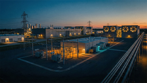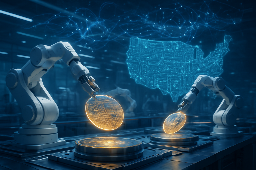
As of December 18, 2025, the landscape of American semiconductor manufacturing has transitioned from a series of ambitious legislative promises into a tangible, operational reality. The CHIPS and Science Act, once a theoretical framework for industrial policy, has reached a critical inflection point where the first "made-in-USA" advanced logic wafers are finally rolling off production lines in Arizona and Texas. This milestone marks the most significant shift in global hardware production in three decades, as the United States attempts to claw back its share of the leading-edge foundry market from Asian giants.
The final quarter of 2025 has seen a dramatic evolution in how these domestic projects are managed. Following the establishment of the U.S. Investment Accelerator earlier this year, the federal government has pivoted from a traditional grant-based system to a "venture-capital style" model. This includes the high-profile finalization of a 9.9% equity stake in Intel (NASDAQ: INTC), funded through a combination of remaining CHIPS grants and the "Secure Enclave" program. By becoming a shareholder in its national champion, the U.S. government has signaled that domestic AI sovereignty is no longer just a matter of policy, but a direct national investment.
High-Volume 18A and the Yield Challenge
The technical centerpiece of this domestic resurgence is Intel’s 18A (1.8nm) process node, which officially entered high-volume mass production at Fab 52 in Chandler, Arizona, in October 2025. This node represents the first time a U.S. firm has attempted to leapfrog the industry leader, TSMC (NYSE: TSM), by utilizing RibbonFET Gate-All-Around (GAA) architecture and PowerVia backside power delivery ahead of its competitors. Initial internal products, including the "Panther Lake" AI PC processors and "Clearwater Forest" server chips, have successfully powered on, demonstrating that the architecture is functional. However, the technical transition has not been without friction; industry analysts report that 18A yields are currently in a "ramp-up phase," meaning they are predictable but not yet at the commercial efficiency levels seen in mature Taiwanese facilities.
Meanwhile, TSMC’s Arizona Fab 1 has reached steady-state volume production, currently churning out 4nm and 5nm chips for major clients like Apple (NASDAQ: AAPL) and NVIDIA (NASDAQ: NVDA). This facility is already providing the essential "Blackwell" architecture components that power the latest generation of AI data centers. TSMC has also accelerated its timeline for Fab 2, with cleanroom equipment installation now targeting 3nm production by early 2027. This technical progress is bolstered by the deployment of the latest High-NA Extreme Ultraviolet (EUV) lithography machines, which are essential for printing the sub-2nm features required for the next generation of AI accelerators.
The competitive gap is further complicated by Samsung (KRX: 005930), which has pivoted its Taylor, Texas facility to focus exclusively on 2nm production. While the project faced construction delays throughout 2024, the fab is now over 90% complete and is expected to go online in early 2026. A significant development this month was the deepening of the Samsung-Tesla (NASDAQ: TSLA) partnership, with Tesla engineers now occupying dedicated workspace within the Taylor fab to oversee the final qualification of the AI5 and AI6 chips. This "co-location" strategy represents a new technical paradigm where the chip designer and the foundry work in physical proximity to optimize silicon for specific AI workloads.
The Competitive Landscape: Diversification vs. Dominance
The immediate beneficiaries of this domestic capacity are the "fabless" giants who have long been vulnerable to the geopolitical risks of the Taiwan Strait. NVIDIA and AMD (NASDAQ: AMD) are the primary winners, as they can now claim a portion of their supply chain is "on-shored," satisfying both ESG requirements and federal procurement mandates. For NVIDIA, having a secondary source for Blackwell-class chips in Arizona provides a strategic buffer against potential disruptions in East Asia. Microsoft (NASDAQ: MSFT) has also emerged as a key strategic partner for Intel’s 18A node, utilizing the domestic capacity to manufacture its "Maia 2" AI processors, which are central to its Azure AI infrastructure.
However, the competitive implications for major AI labs are nuanced. While the U.S. is adding capacity, TSMC’s home-base operations in Taiwan remain the "gold standard" for yield and cost-efficiency. In late 2025, TSMC Taiwan successfully commenced volume production of its N2 (2nm) node with yields exceeding 70%, a figure that Intel and Samsung are still struggling to match in their U.S. facilities. This creates a two-tiered market: the most cutting-edge, cost-effective silicon still flows from Taiwan, while the U.S. fabs serve as a high-security, "sovereign" alternative for mission-critical and government-adjacent AI applications.
The disruption to existing services is most visible in the automotive and industrial sectors. With the U.S. government now holding equity in domestic foundries, there is increasing pressure for "Buy American" mandates in federal AI contracts. This has forced startups and mid-sized AI firms to re-evaluate their hardware roadmaps, often choosing slightly more expensive domestic-made chips to ensure long-term regulatory compliance. The strategic advantage has shifted from those who have the best design to those who have guaranteed "wafer starts" on American soil, a commodity that remains in high demand and limited supply.
Geopolitical Friction and the Asian Response
The broader significance of the CHIPS Act's 2025 status cannot be overstated; it represents a decoupling of the AI hardware stack that was unthinkable five years ago. This development fits into a larger trend of "techno-nationalism," where computing power is viewed as a strategic resource akin to oil. However, this shift has prompted a fierce response from Asian foundries. In China, SMIC (HKG: 0981) has defied expectations by reaching volume production on its "N+3" 5nm-equivalent node without the use of EUV machines. While their costs are significantly higher and yields lower, the successful release of the Huawei Mate 80 series in late 2025 proves that the U.S. lead in manufacturing is not an absolute barrier to entry.
Furthermore, Japan’s Rapidus has emerged as a formidable "third way" in the semiconductor wars. By successfully launching a 2nm pilot line in Hokkaido this year through an alliance with IBM (NYSE: IBM), Japan is positioning itself to leapfrog the 3nm generation entirely. This highlights a potential concern for the U.S. strategy: while the CHIPS Act has successfully brought manufacturing back to American shores, it has also sparked a global subsidy race. The U.S. now finds itself competing not just with rivals like China, but with allies like Japan and South Korea, who are equally determined to maintain their technological relevance in the AI era.
Comparisons to previous milestones, such as the 1980s semiconductor trade disputes, suggest that we are entering a decade of sustained government intervention in the hardware market. The shift toward equity stakes in companies like Intel suggests that the "free market" era of chip manufacturing is effectively over. The potential concern for the AI industry is that this fragmentation could lead to higher hardware costs and slower innovation cycles as companies navigate a "patchwork" of regional manufacturing requirements rather than a single, globalized supply chain.
The Road to 1nm and the 2030 Horizon
Looking ahead, the next two years will be defined by the race to 1nm and the implementation of "High-NA" EUV technology across all major US sites. Intel’s success or failure in stabilizing 18A yields by mid-2026 will determine if the U.S. can truly claim technical parity with TSMC. If yields improve, we expect to see a surge in external foundry customers moving away from "Taiwan-only" strategies. Conversely, if yields remain low, the U.S. government may be forced to increase its equity stakes or provide further "bridge funding" to prevent its national champions from falling behind.
Near-term developments also include the expansion of advanced packaging facilities. While the CHIPS Act focused heavily on "front-end" wafer fabrication, the "back-end" packaging of AI chips remains a bottleneck. We expect the next round of funding to focus heavily on domestic CoWoS (Chip-on-Wafer-on-Substrate) equivalents to ensure that chips made in Arizona don't have to be sent back to Asia for final assembly. Experts predict that by 2030, the U.S. could account for 20% of global leading-edge production, up from 0% in 2022, provided that the labor shortage in specialized engineering is addressed through updated immigration and education policies.
A New Era for American Silicon
The CHIPS Act update of late 2025 reveals a landscape that is both promising and precarious. The key takeaway is that the "brick and mortar" phase of the U.S. semiconductor resurgence is complete; the factories are built, the machines are humming, and the first chips are in hand. However, the transition from building factories to running them at world-class efficiency is a challenge that money alone cannot solve. The U.S. has successfully bought its way back into the game, but winning the game will require a sustained commitment to yield optimization and workforce development.
In the history of AI, this period will likely be remembered as the moment when the "cloud" was anchored to the ground. The physical infrastructure of AI—the silicon, the power, and the packaging—is being redistributed across the globe, ending the era of extreme geographic concentration. As we move into 2026, the industry will be watching the quarterly yield reports from Arizona and the progress of Samsung’s 2nm pivot in Texas. The silicon renaissance has begun, but the true test of its endurance lies in the wafers that will be etched in the coming months.
This content is intended for informational purposes only and represents analysis of current AI developments.
TokenRing AI delivers enterprise-grade solutions for multi-agent AI workflow orchestration, AI-powered development tools, and seamless remote collaboration platforms.
For more information, visit https://www.tokenring.ai/.