
The semiconductor industry is in the midst of a profound transformation, driven not just by shrinking transistors, but by an accelerating shift towards advanced packaging technologies. Once considered a mere protective enclosure for silicon, packaging has rapidly evolved into a critical enabler of performance, efficiency, and functionality, directly addressing the physical and economic limitations that have begun to challenge traditional transistor scaling, often referred to as Moore's Law. These groundbreaking innovations are now fundamental to powering the next generation of high-performance computing (HPC), artificial intelligence (AI), 5G/6G communications, autonomous vehicles, and the ever-expanding Internet of Things (IoT).
This paradigm shift signifies a move beyond monolithic chip design, embracing heterogeneous integration where diverse components are brought together in a single, unified package. By allowing engineers to combine various elements—such as processors, memory, and specialized accelerators—within a unified structure, advanced packaging facilitates superior communication between components, drastically reduces energy consumption, and delivers greater overall system efficiency. This strategic pivot is not just an incremental improvement; it's a foundational change that is reshaping the competitive landscape and driving the capabilities of nearly every advanced electronic device on the planet.
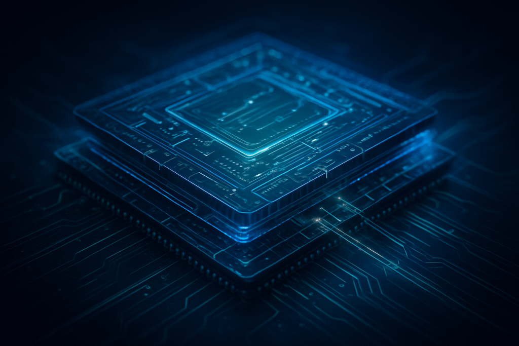
Engineering Brilliance: Diving into the Technical Core of Packaging Innovations
At the heart of this revolution are several sophisticated packaging techniques that are pushing the boundaries of what's possible in silicon design. Heterogeneous integration and chiplet architectures are leading the charge, redefining how complex systems-on-a-chip (SoCs) are conceived. Instead of designing a single, massive chip, chiplets—smaller, specialized dies—can be interconnected within a package. This modular approach offers unprecedented design flexibility, improves manufacturing yields by isolating defects to smaller components, and significantly reduces development costs.
Key to achieving this tight integration are 2.5D and 3D integration techniques. In 2.5D packaging, multiple active semiconductor chips are placed side-by-side on a passive interposer—a high-density wiring substrate, often made of silicon, organic material, or increasingly, glass—that acts as a high-speed communication bridge. 3D packaging takes this a step further by vertically stacking multiple dies or even entire wafers, connecting them with Through-Silicon Vias (TSVs). These vertical interconnects dramatically shorten signal paths, boosting speed and enhancing power efficiency. A leading innovation in 3D packaging is Cu-Cu bumpless hybrid bonding, which creates permanent interconnections with pitches below 10 micrometers, a significant improvement over conventional microbump technology, and is crucial for advanced 3D ICs and High-Bandwidth Memory (HBM). HBM, vital for AI training and HPC, relies on stacking memory dies and connecting them to processors via these high-speed interconnects. For instance, NVIDIA (NASDAQ: NVDA)'s Hopper H200 GPUs integrate six HBM stacks, enabling interconnection speeds of up to 4.8 TB/s.
Another significant advancement is Fan-Out Wafer-Level Packaging (FOWLP) and its larger-scale counterpart, Panel-Level Packaging (FO-PLP). FOWLP enhances standard wafer-level packaging by allowing for a smaller package footprint with improved thermal and electrical performance. It provides a higher number of contacts without increasing die size by fanning out interconnects beyond the die edge using redistribution layers (RDLs), sometimes eliminating the need for interposers or TSVs. FO-PLP extends these benefits to larger panels, promising increased area utilization and further cost efficiency, though challenges in warpage, uniformity, and yield persist. These innovations collectively represent a departure from older, simpler packaging methods, offering denser, faster, and more power-efficient solutions that were previously unattainable. Initial reactions from the AI research community and industry experts are overwhelmingly positive, recognizing these advancements as crucial for the continued scaling of computational power.
Shifting Tides: Impact on AI Companies, Tech Giants, and Startups
The rapid evolution of advanced semiconductor packaging is profoundly reshaping the competitive landscape for AI companies, established tech giants, and nimble startups alike. Companies that master or strategically leverage these technologies stand to gain significant competitive advantages. Foundries like Taiwan Semiconductor Manufacturing Company (NYSE: TSM) and Samsung Electronics Co., Ltd. (KRX: 005930) are at the forefront, heavily investing in proprietary advanced packaging solutions. TSMC's CoWoS (Chip-on-Wafer-on-Substrate) and SoIC (System-on-Integrated-Chips), alongside Samsung's I-Cube and 3.3D packaging, are prime examples of this arms race, offering differentiated services that attract premium customers seeking cutting-edge performance. Intel Corporation (NASDAQ: INTC), with its Foveros and EMIB (Embedded Multi-die Interconnect Bridge) technologies, and its exploration of glass-based substrates, is also making aggressive strides to reclaim its leadership in process and packaging.
These developments have significant competitive implications. Companies like NVIDIA, which heavily rely on HBM and advanced packaging for their AI accelerators, directly benefit from these innovations, enabling them to maintain their performance edge in the lucrative AI and HPC markets. For other tech giants, access to and expertise in these packaging technologies become critical for developing next-generation processors, data center solutions, and edge AI devices. Startups in AI, particularly those focused on specialized hardware or custom silicon, can leverage chiplet architectures to rapidly prototype and deploy highly optimized solutions without the prohibitive costs and complexities of designing a single, massive monolithic chip. This modularity democratizes access to advanced silicon design.
The potential for disruption to existing products and services is substantial. Older, less integrated packaging approaches will struggle to compete on performance and power efficiency. Companies that fail to adapt their product roadmaps to incorporate these advanced techniques risk falling behind. The shift also elevates the importance of the back-end (assembly, packaging, and test) in the semiconductor value chain, creating new opportunities for outsourced semiconductor assembly and test (OSAT) vendors and requiring a re-evaluation of strategic partnerships across the ecosystem. Market positioning is increasingly determined not just by transistor density, but by the ability to intelligently integrate diverse functionalities within a compact, high-performance package, making packaging a strategic cornerstone for future growth and innovation.
A Broader Canvas: Examining Wider Significance and Future Implications
The advancements in semiconductor packaging are not isolated technical feats; they fit squarely into the broader AI landscape and global technology trends, serving as a critical enabler for the next wave of innovation. As the demands of AI models grow exponentially, requiring unprecedented computational power and memory bandwidth, traditional chip design alone cannot keep pace. Advanced packaging offers a sustainable pathway to continued performance scaling, directly addressing the "memory wall" and "power wall" challenges that have plagued AI development. By facilitating heterogeneous integration, these packaging innovations allow for the optimal integration of specialized AI accelerators, CPUs, and memory, leading to more efficient and powerful AI systems that can handle increasingly complex tasks from large language models to real-time inference at the edge.
The impacts are far-reaching. Beyond raw performance, improved power efficiency from shorter interconnects and optimized designs contributes to more sustainable data centers, a growing concern given the energy footprint of AI. This also extends the battery life of AI-powered mobile and edge devices. However, potential concerns include the increasing complexity and cost of advanced packaging technologies, which could create barriers to entry for smaller players. The manufacturing processes for these intricate packages also present challenges in terms of yield, quality control, and the environmental impact of new materials and processes, although the industry is actively working on mitigating these. Compared to previous AI milestones, such as breakthroughs in neural network architectures or algorithm development, advanced packaging is a foundational hardware milestone that makes those software-driven advancements practically feasible and scalable, underscoring its pivotal role in the AI era.
Looking ahead, the trajectory for advanced semiconductor packaging is one of continuous innovation and expansion. Near-term developments are expected to focus on further refinement of hybrid bonding techniques, pushing interconnect pitches even lower to enable denser 3D stacks. The commercialization of glass-based substrates, offering superior electrical and thermal properties over silicon interposers in certain applications, is also on the horizon. Long-term, we can anticipate even more sophisticated integration of novel materials, potentially including photonics for optical interconnects directly within packages, further reducing latency and increasing bandwidth. Potential applications are vast, ranging from ultra-fast AI supercomputers and quantum computing architectures to highly integrated medical devices and next-generation robotics.
Challenges that need to be addressed include standardizing interfaces for chiplets to foster a more open ecosystem, improving thermal management solutions for ever-denser packages, and developing more cost-effective manufacturing processes for high-volume production. Experts predict a continued shift towards "system-in-package" (SiP) designs, where entire functional systems are built within a single package, blurring the lines between chip and module. The convergence of AI-driven design automation with advanced manufacturing techniques is also expected to accelerate the development cycle, leading to quicker deployment of cutting-edge packaging solutions.
The Dawn of a New Era: A Comprehensive Wrap-Up
In summary, the latest advancements in semiconductor packaging technologies represent a critical inflection point for the entire tech industry. Key takeaways include the indispensable role of heterogeneous integration and chiplet architectures in overcoming Moore's Law limitations, the transformative power of 2.5D and 3D stacking with innovations like hybrid bonding and HBM, and the efficiency gains brought by FOWLP and FO-PLP. These innovations are not merely incremental; they are fundamental enablers for the demanding performance and efficiency requirements of modern AI, HPC, and edge computing.
This development's significance in AI history cannot be overstated. It provides the essential hardware foundation upon which future AI breakthroughs will be built, allowing for the creation of more powerful, efficient, and specialized AI systems. Without these packaging advancements, the rapid progress seen in areas like large language models and real-time AI inference would be severely constrained. The long-term impact will be a more modular, efficient, and adaptable semiconductor ecosystem, fostering greater innovation and democratizing access to high-performance computing capabilities.
In the coming weeks and months, industry observers should watch for further announcements from major foundries and IDMs regarding their next-generation packaging roadmaps. Pay close attention to the adoption rates of chiplet standards, advancements in thermal management solutions, and the ongoing development of novel substrate materials. The battle for packaging supremacy will continue to be a key indicator of competitive advantage and a bellwether for the future direction of the entire semiconductor and AI industries.
This content is intended for informational purposes only and represents analysis of current AI developments.
TokenRing AI delivers enterprise-grade solutions for multi-agent AI workflow orchestration, AI-powered development tools, and seamless remote collaboration platforms.
For more information, visit https://www.tokenring.ai/.