
The semiconductor industry is undergoing its most significant architectural transformation in decades, moving beyond the traditional monolithic chip design to embrace a modular future driven by chiplets and heterogeneous integration. This paradigm shift is not merely an incremental improvement but a fundamental re-imagining of how high-performance computing, artificial intelligence, and next-generation devices will be built. As the physical and economic limits of Moore's Law become increasingly apparent, chiplets and heterogeneous integration offer a critical pathway to continue advancing performance, power efficiency, and functionality, heralding a new era of innovation in silicon.
This architectural evolution is particularly significant as it addresses the escalating challenges of fabricating increasingly complex and larger chips on a single silicon die. By breaking down intricate functionalities into smaller, specialized "chiplets" and then integrating them into a single package, manufacturers can achieve unprecedented levels of customization, yield improvements, and performance gains. This strategy is poised to unlock new capabilities across a vast array of applications, from cutting-edge AI accelerators to robust data center infrastructure and advanced mobile platforms, fundamentally altering the competitive landscape for chip designers and technology giants alike.
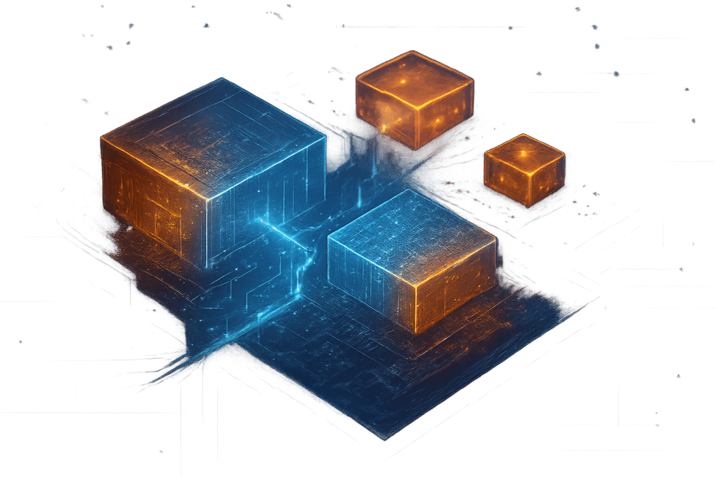
A Modular Revolution: Unpacking the Technical Core of Chiplet Design
At its heart, the rise of chiplets represents a departure from the monolithic System-on-Chip (SoC) design, where all functionalities—CPU cores, GPU, memory controllers, I/O—are squeezed onto a single piece of silicon. While effective for decades, this approach faces severe limitations as transistor sizes shrink and designs grow more complex, leading to diminishing returns in terms of cost, yield, and power. Chiplets, in contrast, are smaller, self-contained functional blocks, each optimized for a specific task (e.g., a CPU core, a GPU tile, a memory controller, an I/O hub).
The true power of chiplets is unleashed through heterogeneous integration (HI), which involves assembling these diverse chiplets—often manufactured using different, optimal process technologies—into a single, advanced package. This integration can take various forms, including 2.5D integration (where chiplets are placed side-by-side on an interposer, effectively a silicon bridge) and 3D integration (where chiplets are stacked vertically, connected by through-silicon vias, or TSVs). This multi-die approach allows for several critical advantages:
- Improved Yield and Cost Efficiency: Manufacturing smaller chiplets significantly increases the likelihood of producing defect-free dies, boosting overall yield. This allows for the use of advanced, more expensive process nodes only for the most performance-critical chiplets, while other components can be fabricated on more mature, cost-effective nodes.
- Enhanced Performance and Power Efficiency: By allowing each chiplet to be designed and fabricated with the most suitable process technology for its function, overall system performance can be optimized. The close proximity of chiplets within advanced packages, facilitated by high-bandwidth, low-latency interconnects, dramatically reduces signal travel time and power consumption compared to traditional board-level interconnections.
- Greater Scalability and Customization: Chiplets enable a "lego-block" approach to chip design. Designers can mix and match various chiplets to create highly customized solutions tailored to specific performance, power, and cost requirements for diverse applications, from high-performance computing (HPC) to edge AI.
- Overcoming Reticle Limits: Monolithic designs are constrained by the physical size limits of lithography reticles. Chiplets bypass this by distributing functionality across multiple smaller dies, allowing for the creation of systems far larger and more complex than a single, monolithic chip could achieve.
Initial reactions from the AI research community and industry experts have been overwhelmingly positive, recognizing chiplets and heterogeneous integration as the definitive path forward for scaling performance in the post-Moore's Law era. The establishment of industry standards like the Universal Chiplet Interconnect Express (UCIe), backed by major players, further solidifies this shift, ensuring interoperability and fostering a robust ecosystem for chiplet-based designs. This collaborative effort is crucial for enabling a future where chiplets from different vendors can seamlessly communicate within a single package, driving innovation and competition.
Reshaping the Competitive Landscape: Strategic Implications for Tech Giants and Startups
The strategic implications of chiplets and heterogeneous integration are profound, fundamentally reshaping the competitive dynamics across the AI and semiconductor industries. This modular approach empowers certain players, disrupts traditional market structures, and creates new avenues for innovation, particularly for those at the forefront of AI development.
Advanced Micro Devices (NASDAQ: AMD) stands out as a pioneer and significant beneficiary of this architectural shift. Having embraced chiplets in its Ryzen and EPYC processors since 2017/2019, and more recently in its Instinct MI300A and MI300X AI accelerators, AMD has demonstrated the cost-effectiveness and flexibility of the approach. By integrating CPU, GPU, FPGA, and high-bandwidth memory (HBM) chiplets onto a single substrate, AMD can offer highly customized and scalable solutions for a wide range of AI workloads, providing a strong competitive alternative to NVIDIA in segments like large language model inference. This strategy has allowed AMD to achieve higher yields and lower marginal costs, bolstering its market position.
Intel Corporation (NASDAQ: INTC) is also heavily invested in chiplet technology through its ambitious IDM 2.0 strategy. Leveraging advanced packaging technologies like Foveros and EMIB, Intel is deploying multiple "tiles" (chiplets) in its Meteor Lake and upcoming Arrow Lake processors for different functions. This allows for CPU and GPU performance scaling by upgrading or swapping individual chiplets rather than redesigning an entire monolithic processor. Intel's Programmable Solutions Group (PSG) has utilized chiplets in its Agilex FPGAs since 2016, and the company is actively fostering a broader ecosystem through its "Chiplet Alliance" with industry leaders like Ansys, Arm, Cadence, Siemens, and Synopsys. A notable partnership with NVIDIA Corporation (NASDAQ: NVDA) to build x86 SoCs integrating NVIDIA RTX GPU chiplets for personal computing further underscores this collaborative and modular future.
While NVIDIA has historically focused on maximizing performance through monolithic designs for its high-end GPUs, the company is also making a strategic pivot. Its Blackwell platform, featuring the B200 chip with two chiplets for its 208 billion transistors, marks a significant step towards a chiplet-based future. As lithographic limits are reached, even NVIDIA, the dominant force in AI acceleration, recognizes the necessity of chiplets to continue pushing performance boundaries, exploring designs with specialized accelerator chiplets for different workloads.
Beyond traditional chipmakers, hyperscalers like Alphabet Inc. (NASDAQ: GOOGL) (Google), Amazon.com, Inc. (NASDAQ: AMZN) (AWS), and Microsoft Corporation (NASDAQ: MSFT) are making substantial investments in designing their own custom AI chips. Google's Tensor Processing Units (TPUs), Amazon's Graviton, Inferentia, and Trainium chips, and Microsoft's custom AI silicon all leverage heterogeneous integration to optimize for their specific cloud workloads. This vertical integration allows these tech giants to tightly optimize hardware with their software stacks and cloud infrastructure, reducing reliance on external suppliers and offering improved price-performance and lower latency for their machine learning services.
The competitive landscape is further shaped by the critical role of foundry and packaging providers like Taiwan Semiconductor Manufacturing Company (NYSE: TSM) (TSMC) with its CoWoS technology, and Intel Foundry Services (IFS) with EMIB/Foveros. These companies provide the advanced manufacturing capabilities and packaging technologies essential for heterogeneous integration. Electronic Design Automation (EDA) companies such as Synopsys, Cadence, and Ansys are also indispensable, offering the tools required to design and verify these complex multi-die systems. For startups, chiplets present both immense opportunities and challenges. While the high cost of advanced packaging and access to cutting-edge fabs remain hurdles, chiplets lower the barrier to entry for designing specialized silicon. Startups can now focus on creating highly optimized chiplets for niche AI functions or developing innovative interconnect technologies, fostering a vibrant ecosystem of specialized IP and accelerating hardware development cycles for specific, smaller volume applications without the prohibitive costs of a full monolithic SoC.
A Foundational Shift for AI: Broader Significance and Historical Parallels
The architectural revolution driven by chiplets and heterogeneous integration extends far beyond mere silicon manufacturing; it represents a foundational shift that will profoundly influence the trajectory of Artificial Intelligence. This paradigm is crucial for sustaining the rapid pace of AI innovation in an era where traditional scaling benefits are diminishing, echoing and, in some ways, surpassing the impact of previous hardware breakthroughs.
This development squarely addresses the challenges of the "More than Moore" era. For decades, AI progress was intrinsically linked to Moore's Law—the relentless doubling of transistors on a chip. As physical limits are reached, chiplets offer an alternative pathway to performance gains, focusing on advanced packaging and integration rather than solely on transistor density. This redefines how computational power is achieved, moving from monolithic scaling to modular optimization. The ability to integrate diverse functionalities—compute, memory, I/O, and even specialized AI accelerators—into a single package with high-bandwidth, low-latency interconnects directly tackles the "memory wall" problem, a critical bottleneck for data-intensive AI workloads by saving significant I/O power and boosting throughput.
The significance of chiplets for AI can be compared to the GPU revolution of the mid-2000s. Originally designed for graphics rendering, GPUs proved exceptionally adept at the parallel computations required for neural network training, catalyzing the deep learning boom. Similarly, the rise of specialized AI accelerators like Google's (NASDAQ: GOOGL) Tensor Processing Units (TPUs) further optimized hardware for specific deep learning tasks. Chiplets extend this trend by enabling even finer-grained specialization. Instead of a single, large AI accelerator, multiple specialized AI chiplets can be combined, each tailored for different aspects or layers of a neural network (e.g., convolution, activation, attention mechanisms). This allows for a bespoke approach to AI hardware, providing unparalleled customization and efficiency for increasingly complex and diverse AI models.
However, this transformative shift is not without its challenges. Standardization remains a critical concern; while initiatives like the Universal Chiplet Interconnect Express (UCIe) aim to foster interoperability, proprietary die-to-die interconnects still complicate a truly open chiplet ecosystem. The design complexity of optimizing power, thermal efficiency, and routing in multi-die architectures demands advanced Electronic Design Automation (EDA) tools and co-design methodologies. Furthermore, manufacturing costs for advanced packaging, coupled with intricate thermal management and power delivery requirements for densely integrated systems, present significant engineering hurdles. Security also emerges as a new frontier of concern, with chiplet-based designs introducing potential vulnerabilities related to hardware Trojans, cross-die side-channel attacks, and intellectual property theft across a more distributed supply chain. Despite these challenges, the ability of chiplets to provide increased performance density, energy efficiency, and unparalleled customization makes them indispensable for the next generation of AI, particularly for the immense computational demands of large generative models and the diverse requirements of multimodal and agentic AI.
The Road Ahead: Future Developments and the AI Horizon
The trajectory of chiplets and heterogeneous integration points towards an increasingly modular and specialized future for computing, with profound implications for AI. This architectural shift is not a temporary trend but a long-term strategic direction for the semiconductor industry, promising continued innovation well beyond the traditional limits of silicon scaling.
In the near-term (1-5 years), we can expect the widespread adoption of advanced packaging technologies like 2.5D and 3D hybrid bonding to become standard practice for high-performance AI and HPC systems. The Universal Chiplet Interconnect Express (UCIe) standard will solidify its position, facilitating greater interoperability and fostering a more open chiplet ecosystem. This will accelerate the development of truly modular AI systems, where specialized compute, memory, and I/O chiplets can be flexibly combined. Concurrently, significant advancements in power distribution networks (PDNs) and thermal management solutions will be crucial to handle the increasing integration density. Intriguingly, AI itself will play a pivotal role, with AI-driven design automation tools becoming indispensable for optimizing IC layout and achieving optimal power, performance, and area (PPA) in complex chiplet-based designs.
Looking further into the long-term, the industry is poised for fully modular semiconductor designs, with custom chiplets optimized for specific AI workloads dominating future architectures. The transition from 2.5D to more prevalent 3D heterogeneous computing, featuring tightly integrated compute and memory stacks, will become commonplace, driven by Through-Silicon Vias (TSVs) and advanced hybrid bonding. A significant breakthrough will be the widespread integration of Co-Packaged Optics (CPO), directly embedding optical communication into packages. This will offer significantly higher bandwidth and lower transmission loss, effectively addressing the persistent "memory wall" challenge for data-intensive AI. Furthermore, the ability to integrate diverse and even incompatible semiconductor materials (e.g., GaN, SiC) will expand the functionality of chiplet-based systems, enabling novel applications.
These developments will unlock a vast array of potential applications and use cases. For Artificial Intelligence (AI) and Machine Learning (ML), custom chiplets will be the bedrock for handling the escalating complexity of large language models (LLMs), computer vision, and autonomous driving, allowing for tailored configurations that optimize performance and energy efficiency. High-Performance Computing (HPC) will benefit from larger-scale integration and modular designs, enabling more powerful simulations and scientific research. Data centers and cloud computing will leverage chiplets for high-performance servers, network switches, and custom accelerators, addressing the insatiable demand for memory and compute. Even edge computing, 5G infrastructure, and advanced automotive systems will see innovations driven by the ability to create efficient, specialized designs for resource-constrained environments.
However, the path forward is not without its challenges. Ensuring efficient, low-latency, and high-bandwidth interconnects between chiplets remains paramount, as different implementations can significantly impact power and performance. The full realization of a multi-vendor chiplet ecosystem hinges on the widespread adoption of robust standardization efforts like UCIe. The inherent design complexity of multi-die architectures demands continuous innovation in EDA tools and co-design methodologies. Persistent issues around power and thermal management, quality control, mechanical stress from heterogeneous materials, and the increased supply chain complexity with associated security risks will require ongoing research and engineering prowess.
Despite these hurdles, expert predictions are overwhelmingly positive. Chiplets are seen as an inevitable evolution, poised to be found in almost all high-performance computing systems, crucial for reducing inter-chip communication power and achieving necessary memory bandwidth. They are revolutionizing AI hardware by driving the demand for specialized and efficient computing architectures, breaking the memory wall for generative AI, and accelerating innovation by enabling faster time-to-market through modular reuse. This paradigm shift fundamentally redefines how computing systems, especially for AI and HPC, are designed and manufactured, promising a future of modular, high-performance, and energy-efficient computing that continues to push the boundaries of what AI can achieve.
The New Era of Silicon: A Comprehensive Wrap-up
The ascent of chiplets and heterogeneous integration marks a definitive turning point in the semiconductor industry, fundamentally redefining how high-performance computing and artificial intelligence systems are conceived, designed, and manufactured. This architectural pivot is not merely an evolutionary step but a revolutionary leap, crucial for navigating the post-Moore's Law landscape and sustaining the relentless pace of AI innovation.
Key Takeaways from this transformation are clear: the future of chip design is inherently modular, moving beyond monolithic structures to a "mix-and-match" strategy of specialized chiplets. This approach unlocks significant performance and power efficiency gains, vital for the ever-increasing demands of AI workloads, particularly large language models. Heterogeneous integration is paramount for AI, allowing the optimal combination of diverse compute types (CPU, GPU, AI accelerators) and high-bandwidth memory (HBM) within a single package. Crucially, advanced packaging has emerged as a core architectural component, no longer just a protective shell. While immensely promising, the path forward is lined with challenges, including establishing robust interoperability standards, managing design complexity, addressing thermal and power delivery hurdles, and securing an increasingly distributed supply chain.
In the grand narrative of AI history, this development stands as a pivotal milestone, comparable in impact to the invention of the transistor or the advent of the GPU. It provides a viable pathway beyond Moore's Law, enabling continued performance scaling when traditional transistor shrinkage falters. Chiplets are indispensable for enabling HBM integration, effectively breaking the "memory wall" that has long constrained data-intensive AI. They facilitate the creation of highly specialized AI accelerators, optimizing for specific tasks with unparalleled efficiency, thereby fueling advancements in generative AI, autonomous systems, and edge computing. Moreover, by allowing for the reuse of validated IP and mixing process nodes, chiplets democratize access to high-performance AI hardware, fostering cost-effective innovation across the industry.
Looking to the long-term impact, chiplet-based designs are poised to become the new standard for complex, high-performance computing systems, especially within the AI domain. This modularity will be critical for the continued scalability of AI, enabling the development of more powerful and efficient AI models previously thought unimaginable. AI itself will increasingly be leveraged for AI-driven design automation, optimizing chiplet layouts and accelerating production. This paradigm also lays the groundwork for new computing paradigms like quantum and neuromorphic computing, which will undoubtedly leverage specialized computational units. Ultimately, this shift fosters a more collaborative semiconductor ecosystem, driven by open standards and a burgeoning "chiplet marketplace."
In the coming weeks and months, several key indicators will signal the maturity and direction of this revolution. Watch closely for standardization progress from consortia like UCIe, as widespread adoption of interoperability standards is crucial. Keep an eye on advanced packaging innovations, particularly in hybrid bonding and co-packaged optics, which will push the boundaries of integration. Observe the growth of the ecosystem and new collaborations among semiconductor giants, foundries, and IP vendors. The maturation and widespread adoption of AI-assisted design tools will be vital. Finally, monitor how the industry addresses critical challenges in power, thermal management, and security, and anticipate new AI processor announcements from major players that increasingly showcase their chiplet-based and heterogeneously integrated architectures, demonstrating tangible performance and efficiency gains. The future of AI is modular, and the journey has just begun.
This content is intended for informational purposes only and represents analysis of current AI developments.
TokenRing AI delivers enterprise-grade solutions for multi-agent AI workflow orchestration, AI-powered development tools, and seamless remote collaboration platforms.
For more information, visit https://www.tokenring.ai/.