TANAKA Successfully Develops the World's First[1] Manufacturing Technology for Platinum Materials with Nano-Sized Crystal Grains
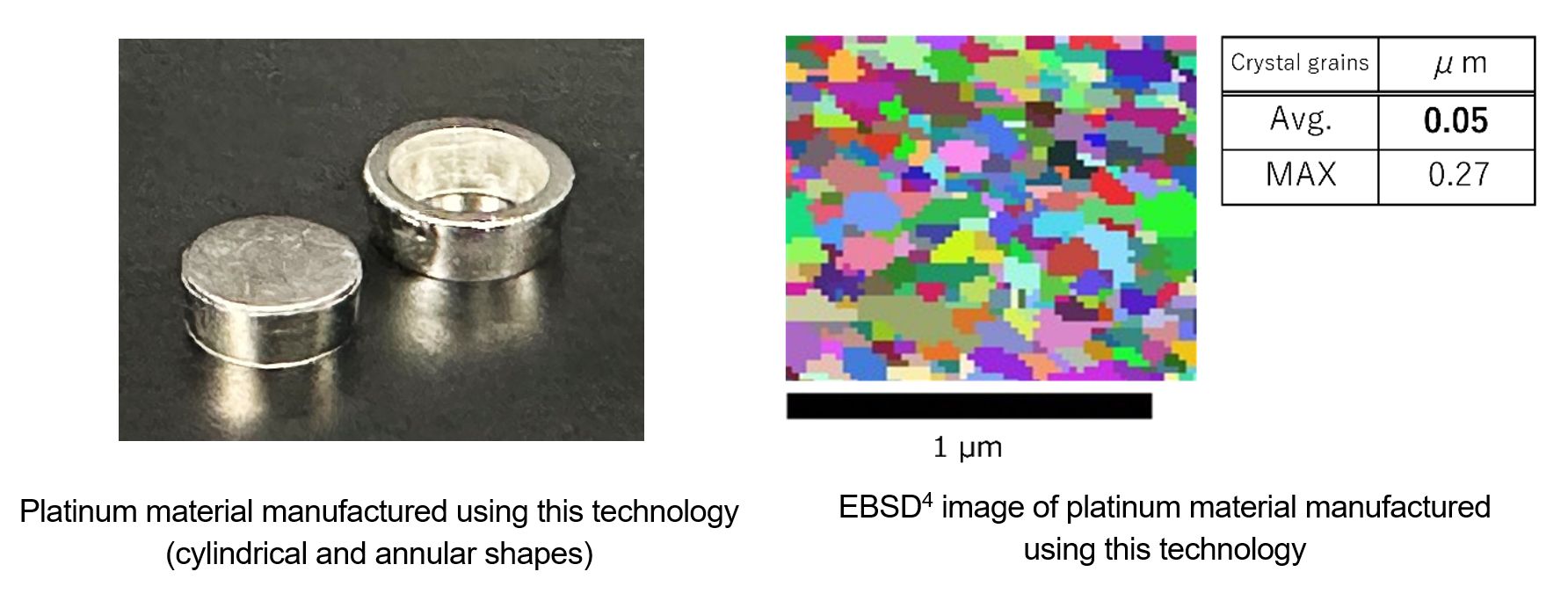
TOKYO, Nov 15, 2024 - (JCN Newswire) - TANAKA Kikinzoku Kogyo K.K. (Head office: Chuo-ku, Tokyo; Representative Director & CEO: Koichiro Tanaka), which develops industrial precious metal products as one of the core companies of TANAKA Precious Metals, announced that it has succeeded in developing the world’s first bulk2 platinum with controlled crystal grain3 size in the nano scale.
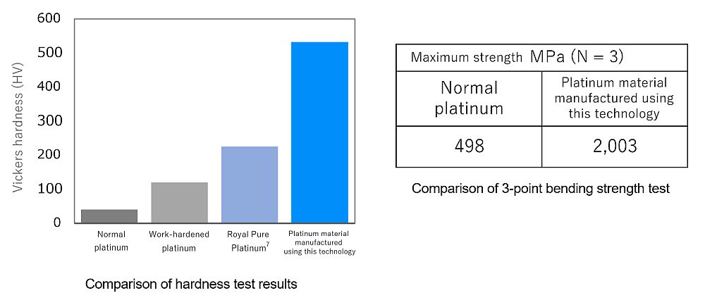
The average grain size of a typical bulk metal is about 10 μm at the smallest. In this new technology, the average crystal grain size can be controlled in the nano scale. As a result, the developed pure platinum, with 99.9% or higher purity, has 10 times the hardness and 4 times the strength of typical platinum materials.
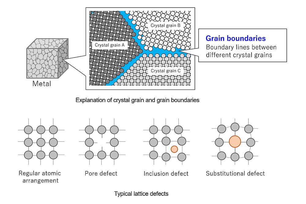
It is known that the properties of metals, including precious metals, are enhanced by grain refinement. In recent years, steel and nonferrous metals with nano-sized crystal grains have been produced by deformation processing to apply extreme levels of plastic deformation5 and recrystallize their structures. While deformation processing temporarily hardens6 metal materials, when highly pure precious metal materials undergo the same process, the arrangement of atoms that form their crystalline structure changes and new crystal grains are nucleated and grown over periods of a few hours to a few days. As a result, the hardness of the material noticeably decreases (softens), and it has been very difficult to refine the crystal grains through deformation processing.
TANAKA Kikinzoku Kogyo has succeeded in manufacturing bulk platinum with controlled crystal grain size in the nano scale by optimizing the manufacturing process. The hardness and strength of the platinum materials manufactured by this technology are much higher than those of typical platinum materials. The developed platinum has a high density of small-angle grain boundaries, large-angle grain boundaries, dislocations, and other lattice defects within the material. Therefore, the developed platinum has properties that are clearly different from the properties of commonly known platinum materials, even without additive elements or alloying. As a new material with high purity and high functionality, it is expected to be applied to a wide field of industries, including the electronics and aerospace industries.
Material Development of Nanostructured Bulk
Many metal materials are polycrystalline, consisting of small crystal grains. It is considered that their properties can be improved by refinement of the crystal grains. The finer the grains, the higher the proportion of grain boundaries or lattice defects, such as dislocations, in the overall material. In materials with nanoscale grain, the ratio of lattice defects is incomparably higher than in commonly known materials, of which the physical properties and characteristics are usually discussed. As a result, unique physical properties and characteristics that are dramatically different from conventional materials are obtained.
1 World’s first: As of October 30, 2024, and based on internal research (according to a survey of patents and papers on bulk platinum materials)
2 Bulky, bulk: Bulky refers to the state of material where clumps of atoms within the material, not on the surface, are connected three-dimensionally. Solid matter with a bulky structure is called bulk.
3 Crystal grains, crystal grain size: Metals have a structure with a regular arrangement of atoms. Crystal grains refer to individual areas of this structure where the orientation of the atomic arrangement is different from neighboring areas, and crystal grain size refers to the diameter of the grains.
4 Electron backscatter diffraction (EBSD): A method of investigating information on material crystals (crystal system, grain size, orientation, etc.) by analyzing the backscatter diffraction from the surface of a material with a crystalline structure when irradiated with an electron beam
5 Plastic deformation: The amount of deformation that remains in a material, without it returning to its original state, after applying an external force to the material to deform it and then removing that external force
6 Work-hardened: The phenomenon of a metal being hardened by applying stress to the metal to accumulate plastic deformation
7 Royal Pure Platinum: An original material manufactured by TANAKA Kikinzoku Kogyo, with higher hardness and strength than normal platinum materials while maintaining a purity of 99.9%
About TANAKA Precious Metals
Since its foundation in 1885, TANAKA Precious Metals has built a portfolio of products to support a diversified range of business uses focused on precious metals. TANAKA is a leader in Japan regarding the volume of precious metals it handles. Over many years, TANAKA has manufactured and sold precious metal products for industry and provided precious metals in such forms as jewelry and assets. As precious metals specialists, all Group companies in Japan and worldwide collaborate on manufacturing, sales, and technology development to offer a full range of products and services. With 5,355 employees, the group’s consolidated net sales for the fiscal year ending December 2023, was 611.1 billion yen.
Global industrial business website
https://tanaka-preciousmetals.com/en/
Product inquiries
TANAKA Kikinzoku Kogyo K.K.
https://tanaka-preciousmetals.com/en/inquiries-on-industrial-products/
Press inquiries
TANAKA Holdings Co., Ltd.
https://tanaka-preciousmetals.com/en/inquiries-for-media/
Press release: http://www.acnnewswire.com/docs/files/20241114_EN.pdf
]]>Source: Tanaka Holdings Co., Ltd.
Copyright 2024 JCN Newswire . All rights reserved.
More News
View More


Recent Quotes
View More
Quotes delayed at least 20 minutes.
By accessing this page, you agree to the Privacy Policy and Terms Of Service.