The Dawn of the Tera-Transistor Era: How Next-Gen Chip Manufacturing is Redefining AI’s Future
By:
TokenRing AI
October 28, 2025 at 15:37 PM EDT
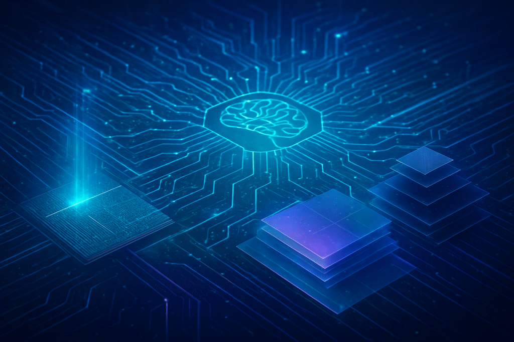
The semiconductor industry is on the cusp of a revolutionary transformation, driven by an insatiable global demand for artificial intelligence and high-performance computing. As the physical limits of traditional silicon scaling (Moore's Law) become increasingly apparent, a trio of groundbreaking advancements – High-Numerical Aperture Extreme Ultraviolet (High-NA EUV) lithography, novel 2D materials, and sophisticated 3D stacking/chiplet architectures – are converging to forge the next generation of semiconductors. These innovations promise to deliver unprecedented processing power, energy efficiency, and miniaturization, fundamentally reshaping the landscape of AI and the broader tech industry for decades to come. This shift marks a departure from solely relying on shrinking transistors on a flat plane. Instead, a holistic approach is emerging, combining ultra-precise patterning, entirely new materials, and modular, vertically integrated designs. The immediate significance lies in enabling the exponential growth of AI capabilities, from massive cloud-based language models to highly intelligent edge devices, while simultaneously addressing critical challenges like power consumption and design complexity. Unpacking the Technological Marvels: A Deep Dive into Next-Gen SiliconThe foundational elements of future chip manufacturing represent significant departures from previous methodologies, each pushing the boundaries of physics and engineering. High-NA EUV Lithography: This is the direct successor to current EUV technology, designed to print features at 2nm nodes and beyond. While existing EUV systems operate with a 0.33 Numerical Aperture (NA), High-NA EUV elevates this to 0.55. This higher NA allows for an 8 nm resolution, a substantial improvement over the 13.5 nm of its predecessor, enabling transistors that are 1.7 times smaller and offering nearly triple the transistor density. The core innovation lies in its larger, anamorphic optics, which require mirrors manufactured to atomic precision over approximately a year. The ASML (AMS: ASML) TWINSCAN EXE:5000, the flagship High-NA EUV system, boasts faster wafer and reticle stages, allowing it to print over 185 wafers per hour. However, the anamorphic optics reduce the exposure field size, necessitating "stitching" for larger dies. This differs from previous DUV (Deep Ultraviolet) and even Low-NA EUV by achieving finer patterns with fewer complex multi-patterning steps, simplifying manufacturing but introducing challenges related to photoresist requirements, stochastic defects, and a reduced depth of focus. Initial industry reactions are mixed; Intel (NASDAQ: INTC) has been an early adopter, receiving the first High-NA EUV modules in December 2023 for its 14A process node, while Taiwan Semiconductor Manufacturing Company (TSMC) (NYSE: TSM) has adopted a more cautious approach, prioritizing cost-efficiency with existing 0.33-NA EUV tools for its A14 node, potentially delaying High-NA EUV implementation until 2030. 2D Materials (e.g., Graphene, MoS2, InSe): These atomically thin materials, just a few atoms thick, offer unique electronic properties that could overcome silicon's physical limits. While graphene, despite high carrier mobility, lacks a bandgap necessary for switching, other 2D materials like Molybdenum Disulfide (MoS2) and Indium Selenide (InSe) are showing immense promise. Recent breakthroughs with wafer-scale 2D indium selenide semiconductors have demonstrated transistors with electron mobility up to 287 cm²/V·s and an average subthreshold swing of 67 mV/dec at room temperature – outperforming conventional silicon transistors and even surpassing the International Roadmap for Devices and Systems (IRDS) performance targets for silicon in 2037. The key difference from silicon is their atomic thinness, which offers superior electrostatic control and resistance to short-channel effects, crucial for sub-nanometer scaling. However, challenges remain in achieving low-resistance contacts, large-scale uniform growth, and integration into existing fabrication processes. The AI research community is cautiously optimistic, with major players like TSMC, Intel, and Samsung (KRX: 005930) investing heavily, recognizing their potential for ultra-high-performance, low-power chips, particularly for neuromorphic and in-sensor computing. 3D Stacking/Chiplet Technology: This paradigm shift moves beyond 2D planar designs by vertically integrating multiple specialized dies (chiplets) into a single package. Chiplets are modular silicon dies, each performing a specific function (e.g., CPU, GPU, memory, I/O), which can be manufactured on different process nodes and then assembled. 3D stacking involves connecting these layers using Through-Silicon Vias (TSVs) or advanced hybrid bonding. This differs from monolithic System-on-Chips (SoCs) by improving manufacturing yield (defects in one chiplet don't ruin the whole chip), enhancing scalability and customization, and accelerating time-to-market. Key advancements include hybrid bonding for ultra-dense vertical interconnects and the Universal Chiplet Interconnect Express (UCIe) standard for efficient chiplet communication. For AI, this means significantly increased memory bandwidth and reduced latency, crucial for data-intensive workloads. Companies like Intel (NASDAQ: INTC) with Foveros and TSMC (NYSE: TSM) with CoWoS are leading the charge in advanced packaging. While offering superior performance and flexibility, challenges include thermal management in densely packed stacks, increased design complexity, and the need for robust industry standards for interoperability. Reshaping the Competitive Landscape: Who Wins in the New Chip Era?These profound shifts in chip manufacturing will have a cascading effect across the tech industry, creating new competitive dynamics and potentially disrupting established market positions. Foundries and IDMs (Integrated Device Manufacturers): Companies like TSMC (NYSE: TSM), Samsung (KRX: 005930), and Intel (NASDAQ: INTC) are at the forefront, directly investing billions in High-NA EUV tools and advanced packaging facilities. Intel's aggressive adoption of High-NA EUV for its 14A process is a strategic move to regain process leadership and attract foundry clients, creating fierce competition, especially against TSMC. Samsung is also rapidly advancing its High-NA EUV and 3D stacking capabilities, aiming for commercial implementation by 2027. Their ability to master these complex technologies will determine their market share and influence over the global semiconductor supply chain. AI Companies (NVIDIA, Google, Microsoft): These companies are the primary beneficiaries, as more advanced and efficient chips are the lifeblood of their AI ambitions. NVIDIA (NASDAQ: NVDA) already leverages 3D stacking with High-Bandwidth Memory (HBM) in its A100/H100 GPUs, and future generations will demand even greater integration and density. Google (NASDAQ: GOOGL) with its TPUs and Microsoft (NASDAQ: MSFT) with its custom Maia AI accelerators will directly benefit from the increased transistor density and power efficiency enabled by High-NA EUV, as well as the customization potential of chiplets. These advancements will allow them to train larger, more complex AI models faster and deploy them more efficiently in cloud data centers and edge devices. Tech Giants (Apple, Amazon): Companies like Apple (NASDAQ: AAPL) and Amazon (NASDAQ: AMZN), which design their own custom silicon, will also leverage these advancements. Apple's M1 Ultra processor already demonstrates the power of 3D stacking by combining two M1 Max chips, enhancing machine learning capabilities. Amazon's custom processors for its cloud infrastructure and edge devices will similarly benefit from chiplet designs, allowing for tailored optimization across its vast ecosystem. Their ability to integrate these cutting-edge technologies into their product lines will be a key differentiator. Startups: While the high cost of High-NA EUV and advanced packaging might seem to favor well-funded giants, chiplet technology offers a unique opportunity for startups. By allowing modular design and the assembly of pre-designed functional blocks, chiplets can lower the barrier to entry for developing specialized AI hardware. Startups focused on novel 2D materials or specific chiplet designs could carve out niche markets. However, access to advanced fabrication and packaging services will remain a critical challenge, potentially leading to consolidation or strategic partnerships. The competitive landscape will shift from pure process node leadership to a broader focus on packaging innovation, material science breakthroughs, and architectural flexibility. Companies that excel in heterogeneous integration and can foster robust chiplet ecosystems will gain a significant strategic advantage, potentially disrupting existing product lines and accelerating the development of highly specialized AI hardware. Wider Implications: AI's March Towards Ubiquity and SustainabilityThe ongoing revolution in chip manufacturing extends far beyond corporate balance sheets, touching upon the broader trajectory of AI, global economics, and environmental sustainability. Fueling the Broader AI Landscape: These advancements are foundational to the continued rapid evolution of AI. High-NA EUV enables the core miniaturization, 2D materials offer radical new avenues for ultra-low power and performance, and 3D stacking/chiplets provide the architectural flexibility to integrate these elements into highly specialized AI accelerators. This synergy will lead to:
Societal Impacts and Potential Concerns:
Comparison to AI Milestones: These manufacturing advancements are as pivotal to the current AI revolution as past breakthroughs were to their respective eras:
The Horizon: What's Next for Chip InnovationThe trajectory of chip manufacturing points towards an increasingly integrated, specialized, and efficient future, driven by relentless innovation and the insatiable demands of AI. Expected Near-Term Developments (1-3 years): Long-Term Developments (5-10+ years): Potential Applications and Use Cases on the Horizon:
Challenges That Need to Be Addressed:
Comprehensive Wrap-Up: A New Era for AI HardwareThe future of chip manufacturing is not merely an incremental step but a profound redefinition of how semiconductors are designed and produced. The confluence of High-NA EUV lithography, revolutionary 2D materials, and advanced 3D stacking/chiplet architectures represents the industry's collective answer to the slowing pace of traditional silicon scaling. These technologies are indispensable for sustaining the rapid growth of artificial intelligence, pushing the boundaries of computational power, energy efficiency, and form factor. The significance of this development in AI history cannot be overstated. Just as the invention of the transistor and the advent of GPUs for deep learning ushered in new eras of computing, these manufacturing advancements are laying the hardware foundation for the next wave of AI breakthroughs. They promise to enable AI systems of unprecedented complexity and capability, from exascale data centers to hyper-intelligent edge devices, making AI truly ubiquitous. However, this transformative journey is not without its challenges. The escalating costs of fabrication, the intricate complexities of integrating diverse technologies, and the critical need for sustainable manufacturing practices will require concerted efforts from industry leaders, academic institutions, and governments worldwide. The geopolitical implications of such concentrated technological power also warrant careful consideration. In the coming weeks and months, watch for announcements from leading foundries like TSMC (NYSE: TSM), Samsung (KRX: 005930), and Intel (NASDAQ: INTC) regarding their High-NA EUV deployments and advancements in hybrid bonding. Keep an eye on research breakthroughs in 2D materials, particularly regarding scalable manufacturing and integration. The evolution of chiplet ecosystems and the adoption of standards like UCIe will also be critical indicators of how quickly this new era of modular, high-performance computing unfolds. The dawn of the tera-transistor era is upon us, promising an exciting, albeit challenging, future for AI and technology as a whole. This content is intended for informational purposes only and represents analysis of current AI developments. TokenRing AI delivers enterprise-grade solutions for multi-agent AI workflow orchestration, AI-powered development tools, and seamless remote collaboration platforms. More NewsView More
The Trade Desk: After a 70% Plunge, This Could Be The Time to Buy ↗
December 04, 2025
Via MarketBeat
Tickers
TTD
Tap Into 2026 AI Infrastructure Gains With This High-Growth ETF ↗
December 04, 2025

Strong Quarter, Weak Reaction: Why GitLab Shares Dropped ↗
December 04, 2025
Via MarketBeat

3 Signs Tesla Is Starting December on the Front Foot ↗
December 04, 2025
Via MarketBeat
Tickers
TSLA
Via MarketBeat
Recent QuotesView More
Stock Quote API & Stock News API supplied by www.cloudquote.io
Quotes delayed at least 20 minutes. By accessing this page, you agree to the Privacy Policy and Terms Of Service.
© 2025 FinancialContent. All rights reserved.
|