Purdue University is spearheading a transformative leap in semiconductor manufacturing, unveiling cutting-edge research that integrates advanced imaging techniques with sophisticated artificial intelligence to detect minuscule defects in chips. This breakthrough promises to revolutionize chip quality, significantly enhance manufacturing efficiency, and bolster the fight against the burgeoning global market for counterfeit components. In an industry where even a defect smaller than a human hair can cripple critical systems, Purdue's innovations offer a crucial safeguard, ensuring the reliability and security of the foundational technology powering our modern world.
This timely development addresses a core challenge in the ever-miniaturizing world of semiconductors: the increasing difficulty of identifying tiny, often invisible, flaws that can lead to catastrophic failures in everything from vehicle steering systems to secure data centers. By moving beyond traditional, often subjective, and time-consuming manual inspections, Purdue's AI-driven approach paves the way for a new standard of precision and speed in chip quality control.
A Technical Deep Dive into Precision and AI
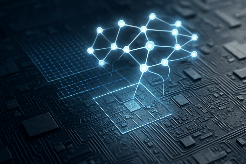
Purdue's research involves a multi-pronged technical approach, leveraging high-resolution imaging and advanced AI algorithms. One key initiative, led by Nikhilesh Chawla, the Ransburg Professor in Materials Engineering, utilizes X-ray imaging and X-ray tomography at facilities like the U.S. Department of Energy's Argonne National Laboratory. This allows researchers to create detailed 3D microstructures of chips, enabling the visualization of even the smallest internal defects and tracing their origins within the manufacturing process. The AI component in this stream focuses on developing efficient algorithms to process this vast imaging data, ensuring rapid, automatic defect identification without impeding the high-volume production lines.
A distinct, yet equally impactful, advancement is the patent-pending optical counterfeit detection method known as RAPTOR (residual attention-based processing of tampered optical responses). Developed by a team led by Alexander Kildishev, a professor in the Elmore Family School of Electrical and Computer Engineering, RAPTOR leverages deep learning to identify tampering by analyzing unique patterns formed by gold nanoparticles embedded on chips. Any alteration to the chip disrupts these patterns, triggering RAPTOR's detection with an impressive 97.6% accuracy rate, even under worst-case scenarios, significantly outperforming previous methods like Hausdorff, Procrustes, and Average Hausdorff distance by substantial margins. Unlike traditional anti-counterfeiting methods that struggle with scalability or distinguishing natural degradation from deliberate tampering, RAPTOR offers robustness against various adversarial features.
These advancements represent a significant departure from previous approaches. Traditional inspection methods, including manual visual checks or rule-based automatic optical inspection (AOI) systems, are often slow, subjective, prone to false positives, and struggle to keep pace with the volume and intricacy of modern chip production, especially as transistors shrink to under 5nm. Purdue's integration of 3D X-ray tomography for internal defects and deep learning for both defect and counterfeit detection offers a non-destructive, highly accurate, and automated solution that was previously unattainable. Initial reactions from the AI research community and industry experts are highly positive, with researchers like Kildishev noting that RAPTOR "opens a large opportunity for the adoption of deep learning-based anti-counterfeit methods in the semiconductor industry," viewing it as a "proof of concept that demonstrates AI's great potential." The broader industry's shift towards AI-driven defect detection, with major players like Taiwan Semiconductor Manufacturing Company (TSMC) (TPE: 2330) reporting significant yield increases (e.g., 20% on 3nm production lines), underscores the transformative potential of Purdue's work.
Industry Implications: A Competitive Edge
Purdue's AI research in semiconductor defect detection stands to profoundly impact a wide array of companies, from chip manufacturers to AI solution providers and equipment makers. Chip manufacturers such as TSMC (TPE: 2330), Samsung Electronics Co., Ltd. (KRX: 005930), and Intel Corporation (NASDAQ: INTC) are poised to be major beneficiaries. By enabling higher yields and reducing waste through automated, highly precise defect detection, these companies can significantly cut costs and accelerate their time-to-market for new products. AI-powered systems can inspect a greater number of wafers with superior accuracy, minimizing material waste and improving the percentage of usable chips. The ability to predict equipment failures through predictive maintenance further optimizes production and reduces costly downtime.
AI inspection solution providers like KLA Corporation (NASDAQ: KLAC) and LandingAI will find immense value in integrating Purdue's advanced AI and imaging techniques into their product portfolios. KLA, known for its metrology and inspection equipment, can enhance its offerings with these sophisticated algorithms, providing more precise solutions for microscopic defect detection. LandingAI, specializing in computer vision for manufacturing, can leverage such research to develop more robust and precise domain-specific Large Vision Models (LVMs) for wafer fabrication, increasing inspection accuracy and delivering faster time-to-value for their clients. These companies gain a competitive advantage by offering solutions that can tackle the increasingly complex defects in advanced nodes.
Semiconductor equipment manufacturers such as ASML Holding N.V. (NASDAQ: ASML), Applied Materials, Inc. (NASDAQ: AMAT), and Lam Research Corporation (NASDAQ: LRCX), while not directly producing chips, will experience an indirect but significant impact. The increased adoption of AI for defect detection will drive demand for more advanced, AI-integrated manufacturing equipment that can seamlessly interact with AI algorithms, provide high-quality data, and even perform real-time adjustments. This could foster collaborative innovation, embedding advanced AI capabilities directly into lithography, deposition, and etching tools. For ASML, whose EUV lithography machines are critical for advanced AI chips, AI-driven defect detection ensures the quality of wafers produced by these complex tools, solidifying its indispensable role.
Major AI companies and tech giants like NVIDIA Corporation (NASDAQ: NVDA) and Intel Corporation (NASDAQ: INTC), both major consumers and developers of advanced chips, benefit from improved chip quality and reliability. NVIDIA, a leader in GPU development for AI, relies on high-quality chips from foundries like TSMC; Purdue's advancements ensure these foundational components are more reliable, crucial for complex AI models and data centers. Intel, as both a designer and manufacturer, can directly integrate this research into its fabrication processes, aligning with its investments in AI for its fabs. This creates a new competitive landscape where differentiation through manufacturing excellence and superior chip quality becomes paramount, compelling companies to invest heavily in AI and computer vision R&D. The disruption to existing products is clear: traditional, less sophisticated inspection methods will become obsolete, replaced by proactive, predictive quality control systems.
Wider Significance: A Pillar of Modern AI
Purdue's AI research in semiconductor defect detection aligns perfectly with several overarching trends in the broader AI landscape, most notably AI for Manufacturing (Industry 4.0) and the pursuit of Trustworthy AI. In the context of Industry 4.0, AI is transforming high-tech manufacturing by bringing unprecedented precision and automation to complex processes. Purdue's work directly contributes to critical quality control and defect detection, which are major drivers for efficiency and reduced waste in the semiconductor industry. This research also embodies the principles of Trustworthy AI by focusing on accuracy, reliability, and explainability in a high-stakes environment, where the integrity of chips is paramount for national security and critical infrastructure.
The impacts of this research are far-reaching. On chip reliability, the ability to detect minuscule defects early and accurately is non-negotiable. AI algorithms, trained on vast datasets, can identify potential weaknesses in chip designs and manufacturing that human eyes or traditional methods would miss, leading to the production of significantly more reliable semiconductor chips. This is crucial as chips become more integrated into critical systems where even minor flaws can have catastrophic consequences. For supply chain security, while Purdue's research primarily focuses on internal manufacturing defects, the enhanced ability to verify the integrity of individual chips before they are integrated into larger systems indirectly strengthens the entire supply chain against counterfeit components, a $75 billion market that jeopardizes safety across aviation, communication, and finance sectors. Economically, the efficiency gains are substantial; AI can reduce manufacturing costs by optimizing processes, predicting maintenance needs, and reducing yield loss—with some estimates suggesting up to a 30% reduction in yield loss and significant operational cost savings.
However, the widespread adoption of such advanced AI also brings potential concerns. Job displacement in inspection and quality control roles is a possibility as automation increases, necessitating a focus on workforce reskilling and new job creation in AI and data science. Data privacy and security remain critical, as industrial AI relies on vast amounts of sensitive manufacturing data, requiring robust governance. Furthermore, AI bias in detection is a risk; if training data is unrepresentative, the AI could perpetuate or amplify biases, leading to certain defect types being consistently missed.
Compared to previous AI milestones in industrial applications, Purdue's work represents a significant evolution. While early expert systems in the 1970s and 80s demonstrated rule-based AI in specific problem-solving, and the machine learning era brought more sophisticated quality control systems (like those at Foxconn or Siemens), Purdue's research pushes the boundaries by integrating high-resolution, 3D imaging (X-ray tomography) with advanced AI for "minuscule defects." This moves beyond simple visual inspection to a more comprehensive, digital-twin-like understanding of chip microstructures and defect formation, enabling not just detection but also root cause analysis. It signifies a leap towards fully autonomous and highly optimized manufacturing, deeply embedding AI into every stage of production.
Future Horizons: The Path Ahead
The trajectory for Purdue's AI research in semiconductor defect detection points towards rapid and transformative future developments. In the near-term (1-3 years), we can expect significant advancements in the speed and accuracy of AI-powered computer vision and deep learning models for defect detection and classification, further reducing false positives. AI systems will become more adept at predictive maintenance, anticipating equipment failures and increasing tool availability. Automated failure analysis will become more sophisticated, and continuous learning models will ensure AI systems become progressively smarter over time, capable of identifying even rare issues. The integration of AI with semiconductor design information will also lead to smarter inspection recipes, optimizing diagnostic processes.
In the long-term (3-10+ years), Purdue's research, particularly through initiatives like the Institute of CHIPS and AI, will contribute to highly sophisticated computational lithography, enabling even smaller and more intricate circuit patterns. The development of hybrid AI models, combining physics-based modeling with machine learning, will lead to greater accuracy and reliability in process control, potentially realizing physics-based, AI-powered "digital twins" of entire fabs. Research into novel AI-specific hardware architectures, such as neuromorphic chips, aims to address the escalating energy demands of growing AI models. AI will also play a pivotal role in accelerating the discovery and validation of new semiconductor materials, essential for future chip designs. Ultimately, the industry is moving towards autonomous semiconductor manufacturing, where AI, IoT, and digital twins will allow machines to detect and resolve process issues with minimal human intervention.
Potential new applications and use cases are vast. AI-driven defect detection will be crucial for advanced packaging, as multi-chip integration becomes more complex. It will be indispensable for the extremely sensitive quantum computing chips, where minuscule flaws can render a chip inoperable. Real-time process control, enabled by AI, will allow for dynamic adjustments of manufacturing parameters, leading to greater consistency and higher yields. Beyond manufacturing, Purdue's RAPTOR technology specifically addresses the critical need for counterfeit chip detection, securing the supply chain.
However, several challenges need to be addressed. The sheer volume and complexity of data generated during semiconductor manufacturing demand highly scalable AI solutions. The computational resources and energy required for training and deploying advanced AI models are significant, necessitating more energy-efficient algorithms and specialized hardware. AI model explainability (XAI) remains a crucial challenge; for critical applications, understanding why an AI identifies a defect is paramount for trust and effective root cause analysis. Furthermore, distinguishing subtle anomalies from natural variations at nanometer scales and ensuring adaptability to new processes and materials without extensive retraining will require ongoing research.
Experts predict a dramatic acceleration in the adoption of AI and machine learning in semiconductor manufacturing, with AI becoming the "backbone of innovation." They foresee AI generating tens of billions in annual value within the next few years, driving the industry towards autonomous operations and a strong synergy between AI-driven chip design and chips optimized for AI. New workforce roles will emerge, requiring continuous investment in education and training, an area Purdue is actively addressing.
A New Benchmark in AI-Driven Manufacturing
Purdue University's pioneering research in integrating cutting-edge imaging and artificial intelligence for detecting minuscule defects in semiconductor chips marks a significant milestone in the history of industrial AI. This development is not merely an incremental improvement but a fundamental shift in how chip quality is assured, moving from reactive, labor-intensive methods to proactive, intelligent, and highly precise automation. The ability to identify flaws at microscopic scales, both internal and external, with unprecedented speed and accuracy, will have a transformative impact on the reliability of electronic devices, the security of global supply chains, and the economic efficiency of one of the world's most critical industries.
The immediate significance lies in the promise of higher yields, reduced manufacturing costs, and a robust defense against counterfeit components, directly benefiting major chipmakers and the broader tech ecosystem. In the long term, this research lays the groundwork for fully autonomous smart fabs, advanced packaging solutions, and the integrity of future technologies like quantum computing. The challenges of data volume, computational resources, and AI explainability will undoubtedly require continued innovation, but Purdue's work demonstrates a clear path forward.
As the world becomes increasingly reliant on advanced semiconductors, the integrity of these foundational components becomes paramount. Purdue's advancements position it as a key player in shaping a future where chips are not just smaller and faster, but also inherently more reliable and secure. What to watch for in the coming weeks and months will be the continued refinement of these AI models, their integration into industrial-scale tools, and further collaborations between academia and industry to translate this groundbreaking research into widespread commercial applications.
This content is intended for informational purposes only and represents analysis of current AI developments.
TokenRing AI delivers enterprise-grade solutions for multi-agent AI workflow orchestration, AI-powered development tools, and seamless remote collaboration platforms. For more information, visit https://www.tokenring.ai/.