- Responding to semiconductor market needs where circuit line widths are becoming increasingly finer -
Dai Nippon Printing Co., Ltd. (DNP) (TOKYO: 7912) has successfully developed a photomask manufacturing process capable of accommodating the 3-nanometer (10-9 meter) lithography process that supports Extreme Ultra-Violet (EUV) lithography, the cutting-edge process for semiconductor manufacturing.
This press release features multimedia. View the full release here: https://www.businesswire.com/news/home/20231205156005/en/
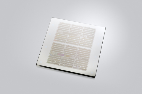
Photomask capable of supporting 3nm EUV lithography (Photo: Business Wire)
[Background]
DNP has continually responded to the demands of semiconductor manufacturers in terms of performance and quality. In 2016, we became the world's first merchant photomask manufacturer to introduce the multi-beam mask writing tool (MBMW). In 2020, we developed a photomask manufacturing process for 5nm EUV lithography processes, and have been supplying masks that meet the needs of the semiconductor market. In this latest development, in order to meet the needs of further miniaturization, we have developed a photomask for EUV lithography capable of supporting 3nm processes.
[Summary]
- MBMW introduced by DNP in 2016 is capable of irradiating with approximately 260,000 electron beams, and can significantly shorten the lithography time even with complex pattern shapes. On this occasion, we have improved the manufacturing process by leveraging the characteristics of the equipment, while optimizing the data correction technology and processing conditions to match the complex curved pattern structure of photomask for EUV lithography.
- DNP has installed a new MBMW, and plans to commence operations in the second half of 2024. We will also strengthen our support for semiconductor manufacturing in advanced areas such as photomasks for EUV lithography.
- DNP will promote joint development of EUV photomasks for next-generation EUV exposure equipment with Interuniversity Microelectronics Center (imec), a cutting-edge international research organization headquartered in Belgium.
[Going Forward]
DNP will provide the newly developed photomask capable of supporting 3nm EUV lithography to semiconductor related manufacturers throughout the world. In addition, we will also support the development of peripheral technologies for EUV lithography, aiming for annual sales of 10 billion yen in 2030.
Through joint development with partners, such as imec, DNP will continue to develop more advanced photomasks capable of supporting processes finer than 3nm and even beyond 2nm.
About DNP
DNP was established in 1876, and has become a leading global company that leverages print-based solutions and the strengths of its growing number of partners to engineer fresh business opportunities while protecting the environment and creating a more vibrant world for all. We capitalize on core competencies in microfabrication and precision coating technology to provide products for the display, electronic device, and optical film markets. We have also developed new products, such as vapor chamber and reflect array that offer next-generation communication solutions for more people-friendly information society.
View source version on businesswire.com: https://www.businesswire.com/news/home/20231205156005/en/
Contacts
Media contact
DNP: Yusuke Kitagawa, 81-3-6735-0101
kitagawa-y3@mail.dnp.co.jp