Thin Wafer Processing and Dicing Equipment Market US$692.5 mn by 2024 – TMR

Transparency Market Research (TMR) estimates that the global thin wafer processing and dicing equipment market has a highly consolidative landscape. Disco Corp. accounted for largest share of 56.4% in 2015 and likely to be dominant in the coming years. This is creating monopoly in the thin wafer processing and dicing equipment market in terms of competitive presence. The other key players such as EV Group, Plasma-Therm LLC, Lam Research Corp, Advanced Dicing Technologies, and Tokyo Electron Ltd. are operating in the global thin wafer processing and dicing equipment market.
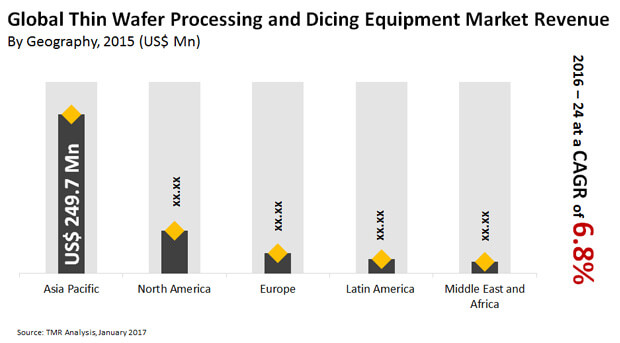
According to TMR, the global thin wafer processing and dicing equipment market is likely to expand at a CAGR of 6.80% over the forecast period to attain a value of US$692.5 mn by 2024-end. The market had acquired a value of US$388.9 mn in 2015.
Request Sample Copy of Report @ https://www.transparencymarketresearch.com/sample/sample.php?flag=S&rep_id=15611
Based on the type, the blade-dicing segment dominated the global thin wafer processing and dicing equipment market and is expected to remain dominant by the end of the forecast period. However, the laser-dicing segment is expected to expand with the fastest CAGR over the predicted years. This growth of the market is attributable to the demand for the high-speed dicing coupled with superior breakage strength.
Based on the region, Asia Pacific accounted for the leading share of 64.2% in 2015 and is anticipated to remain dominant over the forecast period. This growth is due to growing semiconductor manufacturing along with growing industrialization in the region is boosting its adoption. However, North America held the second largest share in the thin wafer processing and dicing equipment market.
Highest Applications in RFID to Propel Market Growth
The thin wafer processing and dicing equipment market is gaining traction due to the incorporation of microelectronics across consumer electronics. The demand for technologies such as power devices and MEMS devices are boosting demand for the thin wafers. Additionally, this demand is boosting demand for better manufacturing processes, which is an important phase in the ultra-thin wafer manufacturing processes.
Immediate Delivery Available | Buy this Premium Research Report – https://www.transparencymarketresearch.com/checkout.php?rep_id=15611<ype=S
Additionally, the thin wafer processing and dicing devices have robust applications among radio-frequency identification devices (RFID) for wafer processing and dicing equipment. Some of the traditional methods are trying to lower the size of the wafer to make it suitable for RFID applications. As RFID requires the thin wafer as thin as 50 to 120 micrometers, the thin wafer processing meets this demand. Growing applications of RFID across identity solutions and consumer electronics is resulting in extensive the growth of the global thin wafer processing and dicing equipment market. Furthermore, RFID has widened its application across smart cards and other identification tags. These applications demand for a smooth surface with the thinned wafer, which is encouraging the use of the thin wafer processing and dicing equipment market.
Investment for Improvement in Wafers to Offer Lucrative Opportunities
Further, growing advancements and lowering size of the wafers is boosting its application across chemical mechanical polishing (CMP). The wafers are increasingly integrated into processing mainly to the high-quality flat surface of the wafer. This is propelling growth of the global thin wafer processing and dicing equipment market. Nonetheless, growing investments for improvement in deposition systems and multiple designs from customers of numerous sectors is offering lucrative opportunities for growth of the thin wafer processing and dicing equipment market. Manufacture of the technologies based on radio frequency (RF) devices supporting to 4G and 5G wireless infrastructure is expected to offer opportunities for growth over the forecast period.
Get Custom Research Report @ https://www.transparencymarketresearch.com/sample/sample.php?flag=CR&rep_id=15611
This information is encompassed in the report by TMR, titled, “Thin Wafer Processing and Dicing Equipment Market (Application – Logic and Memory, Micro Electro Mechanical Systems (MEMS), Power Device, Radio Frequency Identification (RFID), and CMOS Image Sensor; Wafer Thickness – 750 micrometer, 120 micrometer, and 50 micrometer; Dicing Technology – Blade Dicing, Laser Dicing, and Plasma Dicing) – Global Industry Analysis, Trend, Size, Share and Forecast 2016 – 2024.”
Contact Information:
Nikhil Sawlani Transparency Market Research Inc. CORPORATE HEADQUARTER DOWNTOWN, 1000 N. West Street, Suite 1200, Wilmington, Delaware 19801 USA Tel: +1-518-618-1030 USA – Canada Toll-Free: 866-552-345
More News
View More


Recent Quotes
View More
Quotes delayed at least 20 minutes.
By accessing this page, you agree to the Privacy Policy and Terms Of Service.