Phoenix, AZ – September 30, 2025 – Honeywell (NASDAQ: HON) has unveiled a groundbreaking 13MM Pressure Sensor, poised to significantly enhance the efficiency and quality control within the demanding semiconductor manufacturing industry. This innovative technology promises to address critical pain points in wafer fabrication, offering superior precision and purity that could redefine production standards and yield rates. The immediate implications point towards substantial reductions in wafer scrap, optimized process control, and a significant uplift in overall manufacturing reliability, positioning Honeywell as a key enabler in the future of chip production.
The introduction of this advanced sensing solution comes at a pivotal time for the global semiconductor market, which continues to grapple with increasing demand and the relentless pursuit of smaller, more powerful, and more reliable chips. Honeywell's new sensor is designed to operate under the ultra-high purity standards and extreme conditions characteristic of semiconductor facilities, directly tackling issues of contamination and measurement drift that have historically plagued manufacturers. This development is expected to not only streamline production processes but also elevate the consistency and quality of the final semiconductor products, holding considerable sway over the profitability and competitive landscape of the industry.
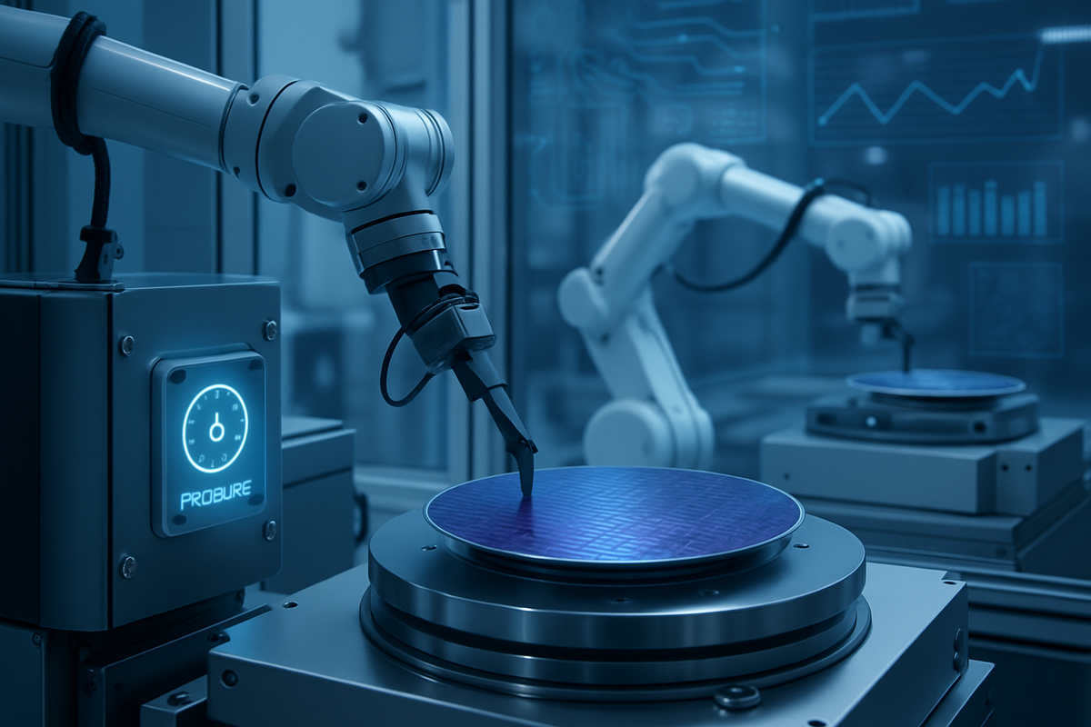
Precision Engineering for a High-Stakes Industry
Honeywell's new 13MM Pressure Sensor is a testament to precision engineering, specifically tailored for the intricate world of semiconductor manufacturing. Its core function is to provide highly accurate and stable pressure measurements across a spectrum of challenging conditions, including vacuum, high-pressure, and high-temperature environments. This capability is crucial for maintaining the exacting standards required in chip fabrication, where even minute deviations can lead to costly defects and compromised product performance. The sensor's design strictly adheres to semiconductor industry standards, such as SEMI F20 for metal composition and surface roughness, ensuring that the sensor itself does not introduce impurities into the production line – a critical factor in achieving ultra-high purity.
The timeline leading up to this release likely involved extensive research and development within Honeywell's advanced materials and sensing divisions, reflecting a strategic focus on high-growth industrial segments. While specific dates for the sensor's conceptualization and testing phases are not publicly detailed, its unveiling on the market suggests a culmination of several years of dedicated innovation. Key players involved in this advancement include Honeywell's internal engineering teams, material scientists, and potentially collaborations with leading semiconductor manufacturers who would have provided critical feedback and validation during the development process. Initial market reactions, though still nascent, are anticipated to be positive, especially from manufacturers keen on improving their yield rates and reducing operational costs. The industry's constant drive for higher efficiency and flawless production makes such a precise and reliable tool highly valuable.
This technology directly impacts the reliability of manufacturing processes by minimizing "drift"—a common measurement instability in vacuum environments. By providing consistent performance, the sensor reduces the need for frequent recalibration and intervention, thereby ensuring smoother, more predictable operations. Furthermore, its compatibility with various gases used in semiconductor manufacturing allows for greater precision in equipment operation, which in turn helps streamline complex manufacturing steps and significantly reduces rework. This comprehensive approach to process control and quality assurance underscores the transformative potential of Honeywell's latest offering.
Market Movers: Winners and Losers in the Semiconductor Race
Honeywell (NASDAQ: HON) itself stands to be a significant winner from the widespread adoption of its new 13MM Pressure Sensor. As a key supplier of critical components and solutions to the industrial sector, this innovation strengthens its position within the high-growth semiconductor equipment market. Increased sales of these advanced sensors will directly contribute to Honeywell's revenue and market share in this specialized niche. Furthermore, the technology enhances Honeywell's reputation as an innovator and a reliable partner for advanced manufacturing, potentially leading to further opportunities in other high-tech industries.
The primary beneficiaries of this technology will be the semiconductor manufacturing companies (fabs) themselves. Large-scale chip manufacturers like Taiwan Semiconductor Manufacturing Company (NYSE: TSM), Intel Corporation (NASDAQ: INTC), and Samsung Electronics (KRX: 005930) stand to gain immensely. By integrating Honeywell's sensors, these companies can expect to see improved wafer yields, reduced scrap rates, and enhanced product quality. This translates directly into higher profitability, greater production efficiency, and a stronger competitive edge in a market where even marginal improvements in yield can mean billions in revenue. Companies specializing in high-performance computing (HPC) and artificial intelligence (AI) chips, which demand the utmost precision and reliability, will find this technology particularly valuable.
Conversely, companies that fail to adopt such advanced sensing technologies might find themselves at a disadvantage. Competitors relying on older, less precise pressure sensors could face higher defect rates, lower yields, and increased operational costs, ultimately impacting their market competitiveness and profitability. This could create pressure on smaller or less agile semiconductor manufacturers to invest in similar upgrades or risk falling behind. Equipment manufacturers who do not integrate such high-purity, high-precision sensors into their offerings for fabs might also see their products become less attractive compared to those that do. While no direct "losers" are immediately evident in terms of company failure, the competitive landscape will certainly shift, favoring those who embrace technological advancements that drive efficiency and quality.
Broader Implications and Industry Trajectories
Honeywell's new sensing technology is not an isolated event but rather a significant development within broader industry trends emphasizing automation, precision, and sustainability in manufacturing. The semiconductor industry, in particular, is under constant pressure to push the boundaries of miniaturization and performance, which necessitates ever-tighter process control and zero-defect manufacturing. This innovation perfectly aligns with the industry's trajectory towards 'lights-out' manufacturing and the increasing adoption of Industry 4.0 principles, where data-driven insights and advanced sensors are critical for optimizing complex production lines.
The ripple effects of this technology could extend across the entire semiconductor supply chain. Equipment manufacturers that integrate these sensors into their tools will offer more competitive products to fabs. Furthermore, the increased efficiency and reduced waste could have positive environmental implications, contributing to the industry's sustainability goals. Partners involved in the supply of ultra-high purity materials and gases will also benefit from the enhanced process control, as their products can be utilized more effectively and with less waste. Historically, advancements in sensing and control technologies have always played a pivotal role in major industrial revolutions, from early factory automation to modern smart manufacturing. This development echoes similar milestones, such as the introduction of advanced metrology tools that enabled the transition to smaller node technologies, setting new benchmarks for precision and quality.
Regulatory bodies are increasingly focusing on the environmental impact of manufacturing, and technologies that reduce waste and energy consumption, like Honeywell's sensor, could be viewed favorably. While there are no immediate direct regulatory implications, the long-term trend towards stricter environmental and quality standards could implicitly reward companies that adopt such advanced, efficiency-boosting solutions. This event highlights the ongoing innovation race within the semiconductor sector, where continuous technological improvements are essential not just for competitive advantage but for the very progression of digital infrastructure worldwide.
The Road Ahead: Opportunities and Challenges
In the short term, the immediate focus will be on the adoption rate of Honeywell's (NASDAQ: HON) 13MM Pressure Sensor by leading semiconductor manufacturers. Successful integration and demonstrated improvements in yield and efficiency will be critical in driving broader market acceptance. This period will present significant opportunities for Honeywell to expand its market reach and establish its technology as an industry standard. For semiconductor fabs, the short-term challenge will be the initial investment and the seamless integration of new sensing technology into existing complex production lines, requiring careful planning and execution to minimize disruption.
Looking further ahead, the long-term possibilities are vast. As semiconductor processes become even more intricate and critical dimensions shrink further, the demand for ultra-precise and reliable sensing will only intensify. This could lead to further iterations and advancements of Honeywell's technology, potentially incorporating AI and machine learning for predictive maintenance and even more sophisticated process control. Strategic pivots for semiconductor manufacturers might involve deeper collaboration with sensor developers to co-create bespoke solutions for future-generation chips. Market opportunities will emerge for companies providing integration services, data analytics platforms that leverage the sensor data, and specialized maintenance for these advanced systems.
Potential scenarios and outcomes include a significant acceleration in the industry's ability to produce next-generation chips with higher yields and lower costs, which would benefit consumers through more affordable and powerful electronic devices. Conversely, a slower-than-expected adoption due to integration complexities or competitive pressures could temper the immediate impact. However, given the relentless pursuit of efficiency and quality in semiconductor manufacturing, the long-term trajectory points towards widespread adoption and continuous innovation in sensing technology, making this a pivotal moment for the industry's future.
A New Era of Precision in Chip Manufacturing
Honeywell's (NASDAQ: HON) introduction of its 13MM Pressure Sensor marks a significant turning point in semiconductor manufacturing, ushering in a new era of precision, efficiency, and quality control. The key takeaway is the direct correlation between this advanced sensing technology and tangible improvements in wafer yield, reduction in costly scrap, and enhanced overall manufacturing reliability. This innovation directly addresses some of the most pressing challenges faced by chipmakers today, offering a clear path to optimized production and a stronger competitive stance in the global market.
Moving forward, the market will closely monitor the rate of adoption and the real-world impact of these sensors on the financial performance of major semiconductor players. Companies that embrace this technology early are likely to gain a significant advantage, translating into higher profitability and a more robust position in the increasingly competitive landscape. The event underscores the continuous need for innovation in foundational industrial technologies to support the rapid advancements in high-tech sectors.
Investors should pay close attention to Honeywell's performance in its industrial and aerospace segments, particularly how this new technology contributes to its revenue streams and market penetration in the semiconductor equipment space. Furthermore, observing the capital expenditure plans and technological upgrade announcements from major semiconductor manufacturers (e.g., Taiwan Semiconductor Manufacturing Company (NYSE: TSM), Intel Corporation (NASDAQ: INTC)) will provide insights into the broader industry's embrace of such precision-enhancing solutions. The lasting impact of this development is likely to be a fundamental shift in how semiconductor purity and process control are achieved, setting new benchmarks for the entire industry for years to come.
This content is intended for informational purposes only and is not financial advice