In a move that signals a seismic shift in the semiconductor landscape, Intel (NASDAQ: INTC) has unveiled a groundbreaking conceptual multi-chiplet package with a massive 10,296 mm² silicon footprint. Roughly 12 times the size of today’s largest AI processors and comparable in dimensions to a modern smartphone, this "super-chip" represents the pinnacle of Intel’s "Systems Foundry" vision. By shattering the traditional lithography reticle limit, Intel is positioning itself to deliver unprecedented AI compute density, aiming to consolidate the power of an entire data center rack into a single, modular silicon entity.
This announcement comes at a critical juncture for the industry, as the demand for Large Language Model (LLM) training and generative AI continues to outpace the physical limits of monolithic chip design. By integrating 16 high-performance compute elements with advanced memory and power delivery systems, Intel is not just manufacturing a processor; it is engineering a complete high-performance computing system on a substrate. The design serves as a direct challenge to the dominance of TSMC (NYSE: TSM), signaling that the race for AI supremacy will be won through advanced 2.5D and 3D packaging as much as through raw transistor scaling.
Technical Breakdown: The 14A and 18A Synergy
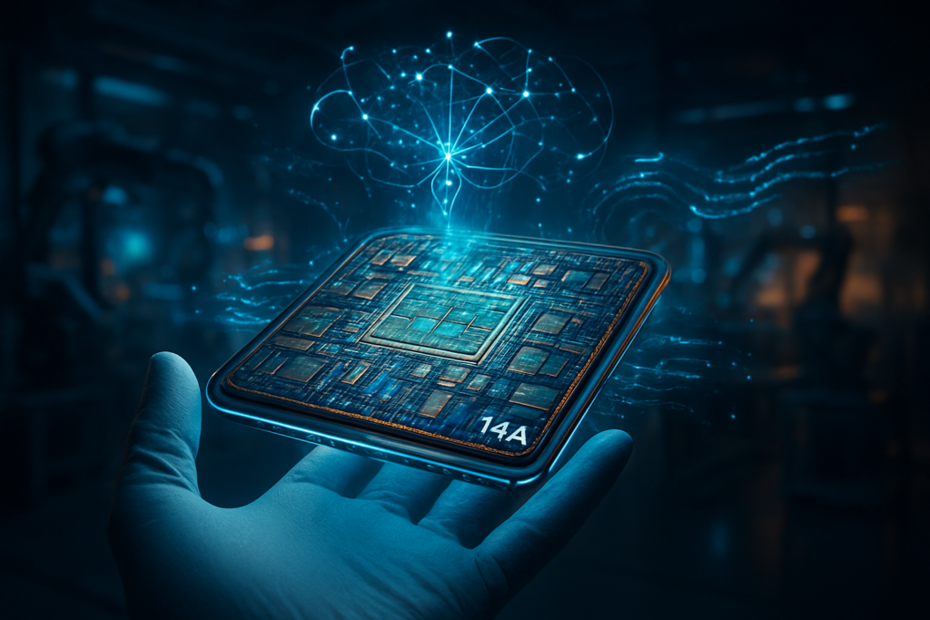
The "smartphone-sized" floorplan is a masterclass in heterogeneous integration, utilizing a mix of Intel’s most advanced process nodes. At the heart of the design are 16 large compute elements produced on the Intel 14A (1.4nm-class) process. These tiles leverage second-generation RibbonFET Gate-All-Around (GAA) transistors and PowerDirect—Intel’s sophisticated backside power delivery system—to achieve extreme logic density and performance-per-watt. By separating the power network from signal routing, Intel has effectively eliminated the "wiring bottleneck" that plagues traditional high-end silicon.
Supporting these compute tiles are eight large base dies manufactured on the Intel 18A-PT node. Unlike the passive interposers used in many current designs, these are active silicon layers packed with massive amounts of embedded SRAM. This architecture, reminiscent of the "Clearwater Forest" design, allows for ultra-low-latency data movement between the compute engines and the memory subsystem. Surrounding this core are 24 HBM5 (High Bandwidth Memory 5) stacks, providing the multi-terabyte-per-second throughput necessary to feed the voracious appetite of the 14A logic array.
To hold this massive 10,296 mm² assembly together, Intel utilizes a "3.5D" packaging approach. This includes Foveros Direct 3D, which enables vertical stacking with a sub-9µm copper-to-copper pitch, and EMIB-T (Embedded Multi-die Interconnect Bridge), which provides high-bandwidth horizontal connections between the base dies and HBM5 modules. This combination allows Intel to overcome the ~830 mm² reticle limit—the physical boundary of what a single lithography pass can print—by stitching multiple reticle-sized regions into a unified, coherent processor.
Strategic Implications for the AI Ecosystem
The unveiling of this design has immediate ramifications for tech giants and AI labs. Intel’s "Systems Foundry" approach is designed to attract hyperscalers like Microsoft (NASDAQ: MSFT) and Amazon (NASDAQ: AMZN), who are increasingly looking to design their own custom silicon. Microsoft has already confirmed its commitment to the Intel 18A process for its future Maia AI processors, and this new 10,000 mm² design provides a blueprint for how those chips could scale into the next decade.
Perhaps the most surprising development is the warming relationship between Intel and NVIDIA (NASDAQ: NVDA). As NVIDIA seeks to diversify its supply chain and hedge against TSMC’s capacity constraints, it has reportedly explored Intel’s Foveros and EMIB packaging for its future Blackwell-successor architectures. The ability to "mix and match" compute dies from various nodes—such as pairing an NVIDIA GPU tile with Intel’s 18A base dies—gives Intel a unique strategic advantage. This flexibility could disrupt the current market positioning where TSMC’s CoWoS (Chip on Wafer on Substrate) is the only viable path for high-end AI hardware.
The Broader AI Landscape and the 5,000W Frontier
This development fits into a broader trend of "system-centric" silicon design. As the industry moves toward Artificial General Intelligence (AGI), the bottleneck has shifted from how many transistors can fit on a chip to how much power and data can be delivered to those transistors. Intel’s design is a "technological flex" that addresses this head-on, with future variants of the Foveros-B packaging rumored to support power delivery of up to 5,000W per module.
However, such massive power requirements raise significant concerns regarding thermal management and infrastructure. Cooling a "smartphone-sized" chip that consumes as much power as five average households will require revolutionary liquid-cooling and immersion solutions. Comparisons are already being drawn to the Cerebras (Private) Wafer-Scale Engine; however, while Cerebras uses an entire monolithic wafer, Intel’s chiplet-based approach offers a more practical path to high yields and heterogeneous integration, allowing for more complex logic configurations than a single-wafer design typically permits.
Future Horizons: From Concept to "Jaguar Shores"
Looking ahead, this 10,296 mm² design is widely considered the precursor to Intel’s next-generation AI accelerator, codenamed "Jaguar Shores." While Intel’s immediate focus remains on the H1 2026 ramp of Clearwater Forest and the stabilization of the 18A node, the 14A roadmap points to a 2027 timeframe for volume production of these massive multi-chiplet systems.
The potential applications for such a device are vast, ranging from real-time global climate modeling to the training of trillion-parameter models in a fraction of the current time. The primary challenge remains execution. Intel must prove it can achieve viable yields on the 14A node and that its EMIB-T interconnects can maintain signal integrity across such a massive physical distance. If successful, the "Jaguar Shores" era could redefine what is possible in the realm of edge-case AI and autonomous research.
A New Chapter in Semiconductor History
Intel’s unveiling of the 10,296 mm² multi-chiplet design marks a pivotal moment in the history of computing. It represents the transition from the era of the "Micro-Processor" to the era of the "System-Processor." By successfully integrating 16 compute elements and HBM5 into a single smartphone-sized footprint, Intel has laid down a gauntlet for TSMC and Samsung, proving that it still possesses the engineering prowess to lead the high-performance computing market.
As we move into 2026, the industry will be watching closely to see if Intel can translate this conceptual brilliance into high-volume manufacturing. The strategic partnerships with NVIDIA and Microsoft suggest that the market is ready for a second major foundry player. If Intel can hit its 14A milestones, this "smartphone-sized" giant may very well become the foundation upon which the next generation of AI is built.
This content is intended for informational purposes only and represents analysis of current AI developments.
TokenRing AI delivers enterprise-grade solutions for multi-agent AI workflow orchestration, AI-powered development tools, and seamless remote collaboration platforms.
For more information, visit https://www.tokenring.ai/.